Organic light emitting diode and method of fabricating the same

a light-emitting diode and organic technology, applied in the direction of discharge tube/lamp details, discharge tube luminescnet screens, organic semiconductor devices, etc., can solve the problems of limiting the efficiency and achieve the effect of increasing the luminance and life span of oleds and facilitating current supply

Active Publication Date: 2011-09-13
SAMSUNG DISPLAY CO LTD
View PDF61 Cites 2 Cited by
  • Summary
  • Abstract
  • Description
  • Claims
  • Application Information

AI Technical Summary

Benefits of technology

[0009]Aspects of embodiments of the present invention are directed toward an organic light emitting diode (OLED) and a method of fabricating the same, which facilitate supply of current to an emission layer to increase the luminance and life span of the OLED.
[0010]Another aspect of an embodiment of the present invention is directed toward an OLED having an intermediate layer formed between a first hole transport layer (HTL) and a second hole transport layer to facilitate supply of current to an emission layer (EML), thereby increasing the luminance and life span of the OLED.

Problems solved by technology

However, the conventional hole injection layer and hole transport layer have a specific technical limit that limits how much the efficiency and life span of the OLEDs can be improved.

Method used


Image

  • Organic light emitting diode and method of fabricating the same
  • Organic light emitting diode and method of fabricating the same
  • Organic light emitting diode and method of fabricating the same

Examples


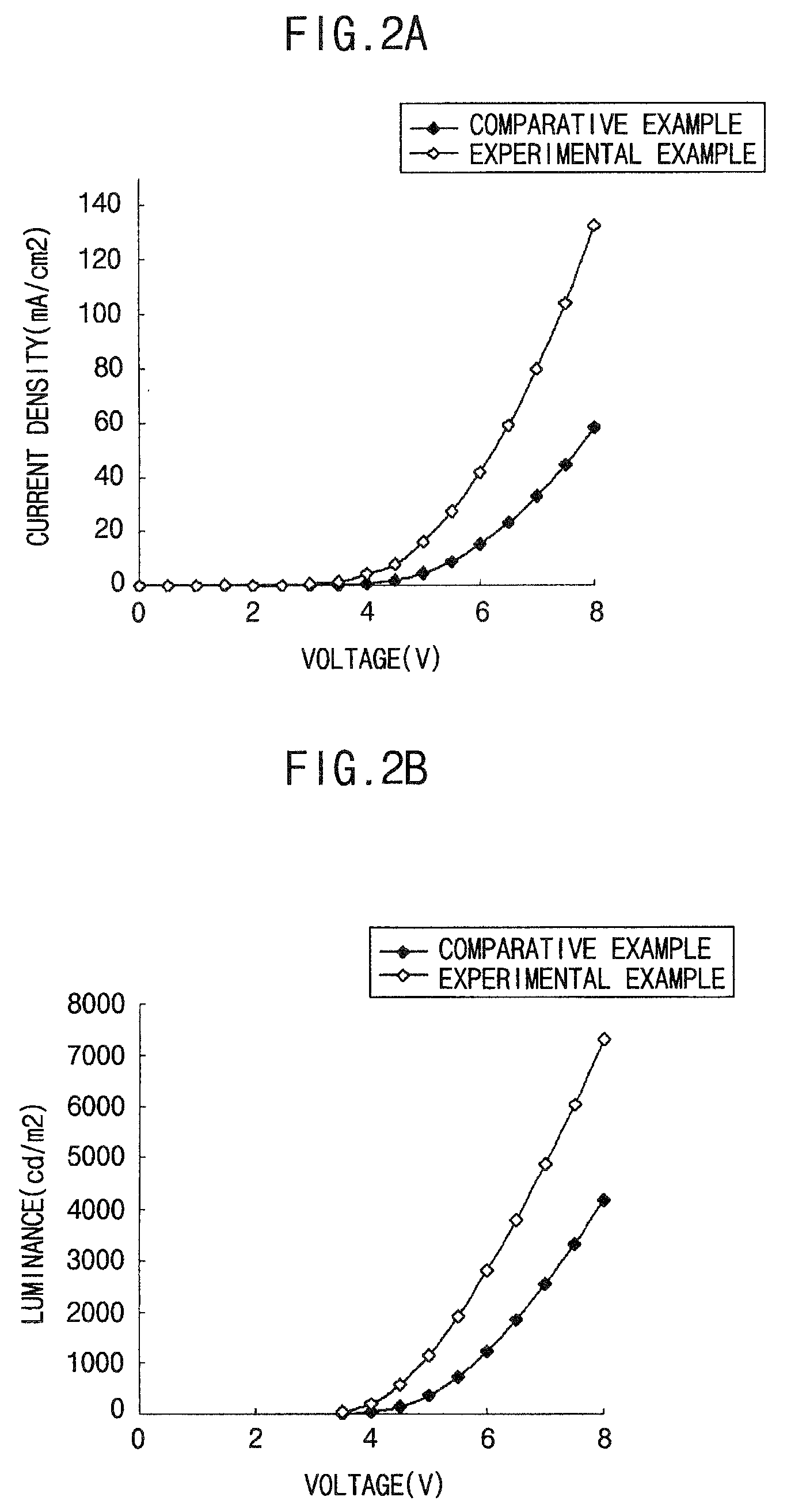
experimental example

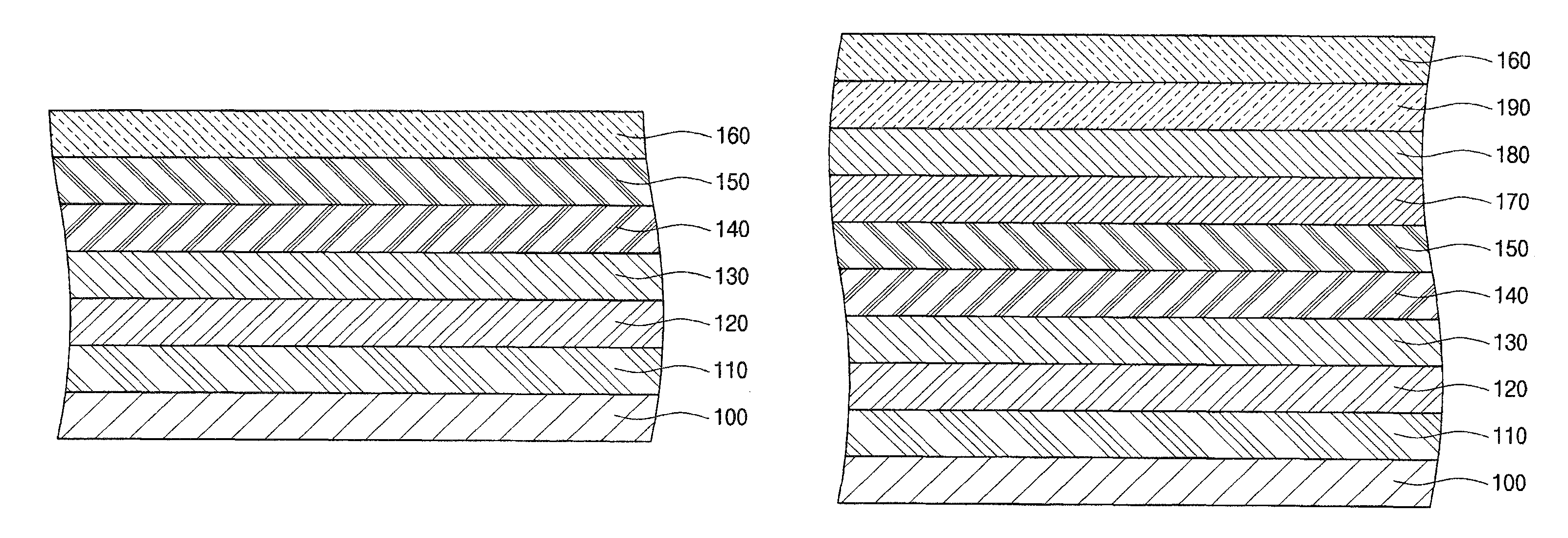
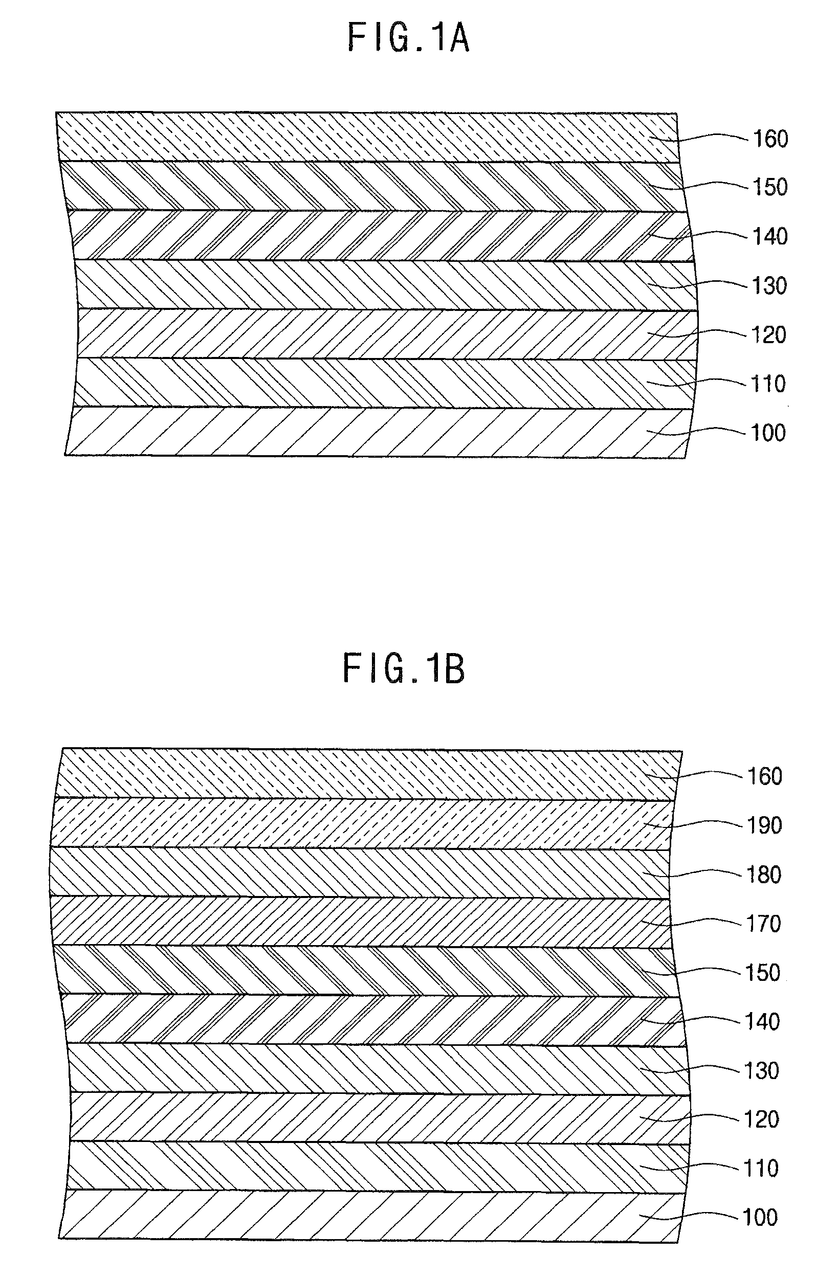
[0040]A first electrode was formed of ITO to a thickness of about 1000 Å. Thereafter, a hole injection layer was formed of mTDATA on the first electrode to a thickness of about 600 Å, and a first hole transport layer was formed of NPB on the hole injection layer to a thickness of about 150 Å. An intermediate layer was formed of MoO3 on the first hole transport layer to a thickness of about 50 Å. A second hole transport layer was formed of NPB on the intermediate layer to a thickness of about 100 Å. A red phosphorescent emission layer was formed on the second hole transport layer utilizing a mixture of CBP, as a host, and 12% by weight of Ir(piq)3, as a dopant, to a thickness of about 300 Å. An electron transport layer was formed of Alq3 on the red phosphorescent emission layer to a thickness of about 350 Å. Subsequently, an electron injection layer was formed of LiF on the electron transport layer to a thickness of about 5 Å. A second electrode was formed of Al on the electron injec...


PUM


Abstract

An organic light emitting diode (OLED) and a method of fabricating the same, in which an intermediate layer is formed between a first hole transport layer (HTL) and a second hole transport layer to facilitate supply of current to an emission layer (EML), thereby increasing the luminance and life span of the OLED. The OLED includes a first electrode, a hole injection layer (HIL) disposed on the first electrode, a first hole transport layer disposed on the hole injection layer, an intermediate layer disposed on the first hole transport layer, a second hole transport layer disposed on the intermediate layer, an emission layer disposed on the second hole transport layer, and a second electrode disposed on the emission layer.

Description

CROSS-REFERENCE TO RELATED APPLICATION[0001]This application claims priority to and the benefit of Korean Patent Application No. 10-2008-17328, filed Feb. 26, 2008, the entire content of which is incorporated herein by reference.BACKGROUND OF THE INVENTION[0002]1. Field of the Invention[0003]The present invention relates to an organic light emitting diode (OLED) and a method of fabricating the same and, more particularly, to an OLED in which an intermediate layer is formed between a first hole transport layer (HTL) and a second hole transport layer.[0004]2. Description of the Related Art[0005]An organic light emitting diode (OLED) is an emissive display that is made ultrathin and lightweight and can be fabricated in a simple process using a small number of components. Also, the OLED has high resolution and a wide viewing angle and is capable of displaying a realistic moving image with high color purity. Furthermore, the OLED can be driven at low power and low voltage and is adequate...

Claims


Application Information

Patent Timeline
Patent Type & Authority Patents(United States)
IPC IPC(8): H01J1/62
CPCH01L51/5088H01L51/0085H01L2251/308H10K85/342H10K50/17H10K2102/103H01L21/28568H10N30/076H10K50/14H10K50/15
Inventor YANG, NAM-CHOUL
Owner SAMSUNG DISPLAY CO LTD
Why Eureka
Try Eureka