Method of manufacturing MEMS device

a manufacturing method and technology of a mems device, applied in the direction of basic electric elements, impedence networks, electric apparatus, etc., can solve the problems of difficult external visual recognition to check directly the etched state, the uniformity of the etching is not easily affected, etc., to achieve accurate control of the etching state, improve the uniformity of the surface etching for the movable portion, and improve the accuracy of the etching

Inactive Publication Date: 2011-09-27
SEIKO EPSON CORP
View PDF9 Cites 19 Cited by
  • Summary
  • Abstract
  • Description
  • Claims
  • Application Information

AI Technical Summary

Benefits of technology

An advantage of some aspects of the invention is that it provides a method of adjusting an MEMS device capable of adjusting the structural size of the MEMS structure over a broad range and performing size adjustment uniformly without changing the operational aspects and a method of manufacturing the MEMS device using the method of adjusting the MEMS device.
According to a method of adjusting an MEMS device and a method of manufacturing an MEMS device by using the adjusting method, there are excellent advantages in that the structural size of the MEMS structure can be adjusted over a broad range, uniform size adjustment can be performed, and a variance in the operational aspects can be avoided.

Problems solved by technology

In addition, since gas-phase etching is used, even when surface etching is performed for the MEMS structure disposed inside the hollow portion of the covering structure, deviation in the uniformity of the etching does not easily occur.
In addition, since the MEMS structure is disposed inside the hollow portion of the covering structure, it is difficult to check directly the etched state by external visual recognition.

Method used


Image

  • Method of manufacturing MEMS device
  • Method of manufacturing MEMS device
  • Method of manufacturing MEMS device

Examples


Embodiment Construction

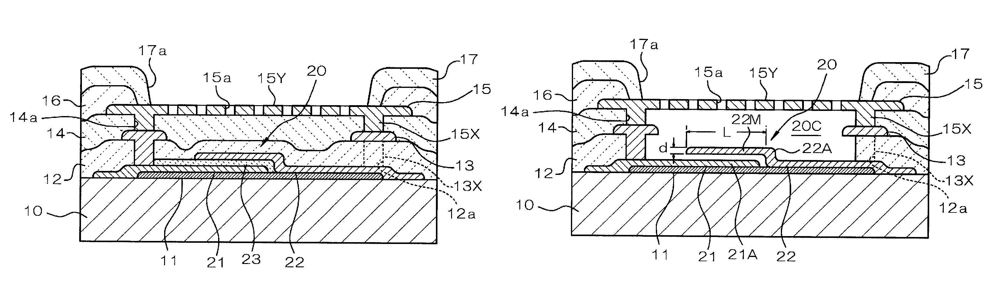
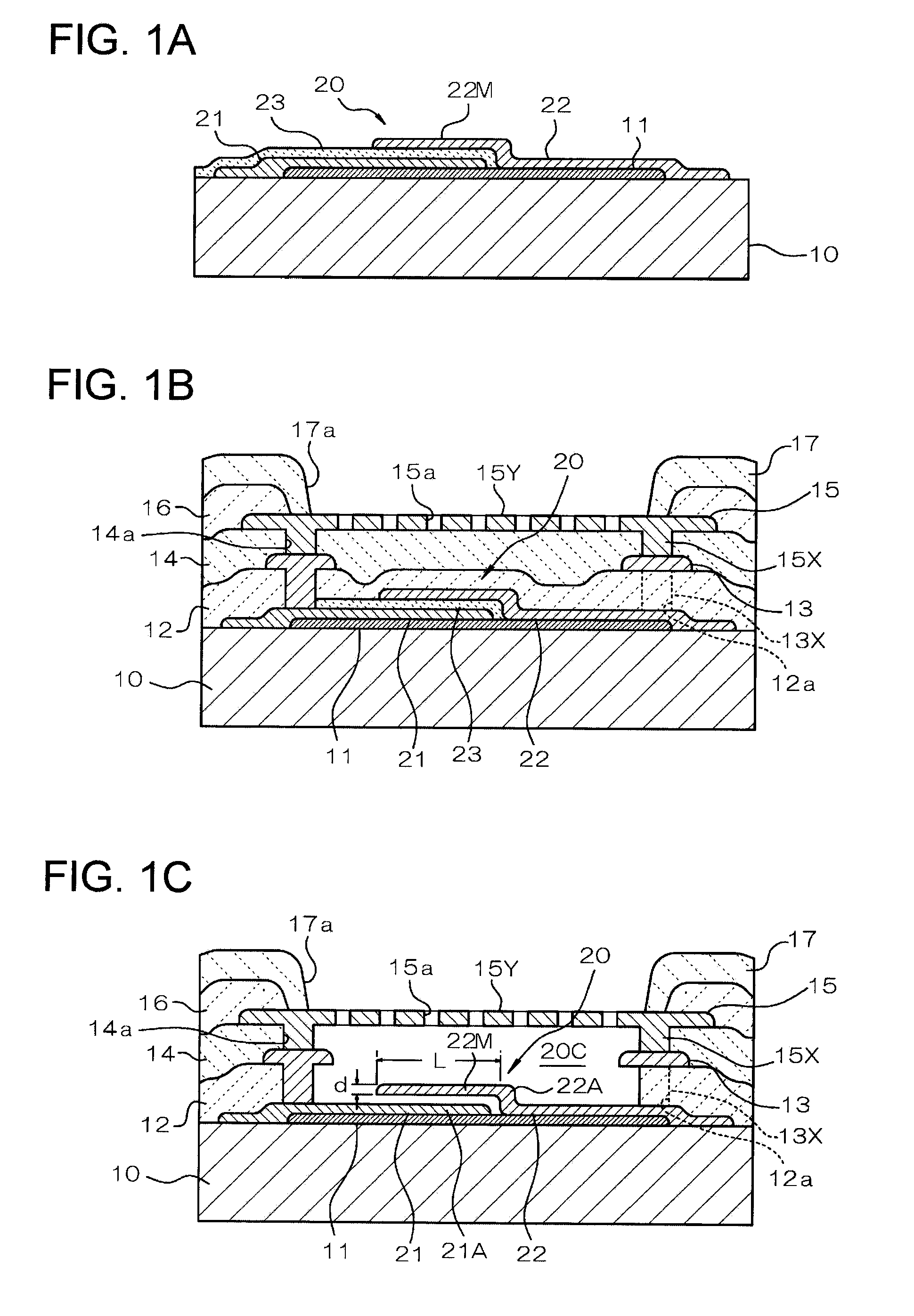
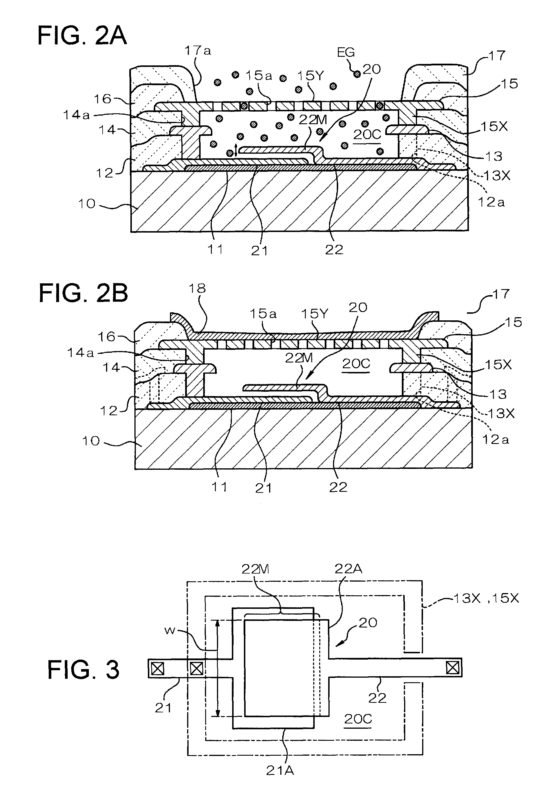
Next, exemplary embodiments of the invention will be described with reference to the accompanying drawings. First, a method of manufacturing an MEMS device according to an embodiment of the invention will be described with reference to FIGS. 1A to 1C and FIGS. 2A and 2B. FIGS. 1A to 1C and FIGS. 2A and 2B are schematic cross-sectional views showing each process of the method of manufacturing the MEMS device according to this embodiment.

As shown in FIG. 1A, in this embodiment, an MEMS device is manufactured which is configured by using a substrate (wafer) 10 formed of a semiconductor such as a single crystalline silicon as a base body and forming an MEMS structure 20 on the substrate 10. However, the substrate 10 is not limited to semiconductor and may be formed from various materials such as glass, ceramics, or resin.

On the surface of the substrate 10, an insulating film (not shown) made from silicon oxide or the like is formed as is necessary, and accordingly, insulation from the s...


PUM


Abstract

A method of manufacturing an MEMS device includes: forming a covering structure having an MEMS structure and a hollow portion, which is located on a periphery of the MEMS structure and is opened to an outside, on a substrate; and performing surface etching for the MEMS structure in a gas phase by supplying an etching gas to the periphery of the MEMS structure from the outside.

Description

BACKGROUND1. Technical FieldThe present invention relates to a method of manufacturing an MEMS device, and more particularly, to a manufacturing process for adjusting the structural size of an MEMS structure.2. Related ArtMEMS (Micro Electro Mechanical Systems) relate to one of the technologies for forming micro structures. For example, MEMS relate to technology for producing a delicate electromechanical system of a micron order or such products. Generally, semiconductor chips have a circuit structure that is a two-dimensional pattern by manufacturing an electronic circuit by stacking thin films such as a silicon film, an oxidation film, and a metal film on a silicon substrate. However, when the technology for manufacturing the semiconductor chip, that is, semiconductor manufacturing technology is used in the MEMS, a leaf spring, a mirror, a rotation shaft, and the like of micron sizes are formed by forming a thin film on a substrate and by partially separating the thin film from th...

Claims


Application Information

Patent Timeline
Patent Type & Authority Patents(United States)
IPC IPC(8): H01L21/00
CPCH03H3/0077H03H9/2457H03H2009/02496H03H2009/02511
Inventor KIHARA, RYUJIINABA, SHOGO
Owner SEIKO EPSON CORP
Why Eureka
Try Eureka