Unlock instant, AI-driven research and patent intelligence for your innovation.

Plasma display device and method of manufacturing green phosphor material for plasma display device

a technology of plasma display device and green phosphor material, which is applied in the direction of luminescent composition, gas-filled discharge tube, chemistry apparatus and processes, etc., can solve the problems of discharge instability, decrease of green luminance, and decrease of zn/sub>2/sub>sio/sub>4/sub>, etc., and achieve small luminance reduction

Inactive Publication Date: 2011-10-11
PANASONIC CORP
View PDF20 Cites 0 Cited by
  • Summary
  • Abstract
  • Description
  • Claims
  • Application Information

AI Technical Summary

Benefits of technology

"The present invention is a PDP device that uses a green phosphor material consisting of Zn2SiO4:Mn. The device has a panel main body with barrier ribs that divide the discharge space into multiple spaces, and a group of electrodes that generate discharge in the divided space. The phosphor layers that emit upon discharge have a high luminance and minimal decrease in luminance even after long hours of use. The technical effect of this invention is to provide a PDP device with improved display quality and durability."

Problems solved by technology

Therefore, when the PDP device is used for a long time, green luminance decreases due to the deterioration of the Zn2SiO4:Mn.
However, because the surface of Zn2SiO4:Mn is coated with a film substance that does not emit in layering films with the vapor deposition method and the firing method, there is a problem that the luminance of Zn2SiO4:Mn decreases.
However, because the metal alkoxide is a compound containing organic substances, a carbon-based compound remains on the phosphor surface if the firing is not performed sufficiently.
In particular, the carbon-based compound decomposed with long hours of use is released in the discharge space, and the discharge becomes unstable.

Method used


Image

  • Plasma display device and method of manufacturing green phosphor material for plasma display device
  • Plasma display device and method of manufacturing green phosphor material for plasma display device
  • Plasma display device and method of manufacturing green phosphor material for plasma display device

Examples


embodiment

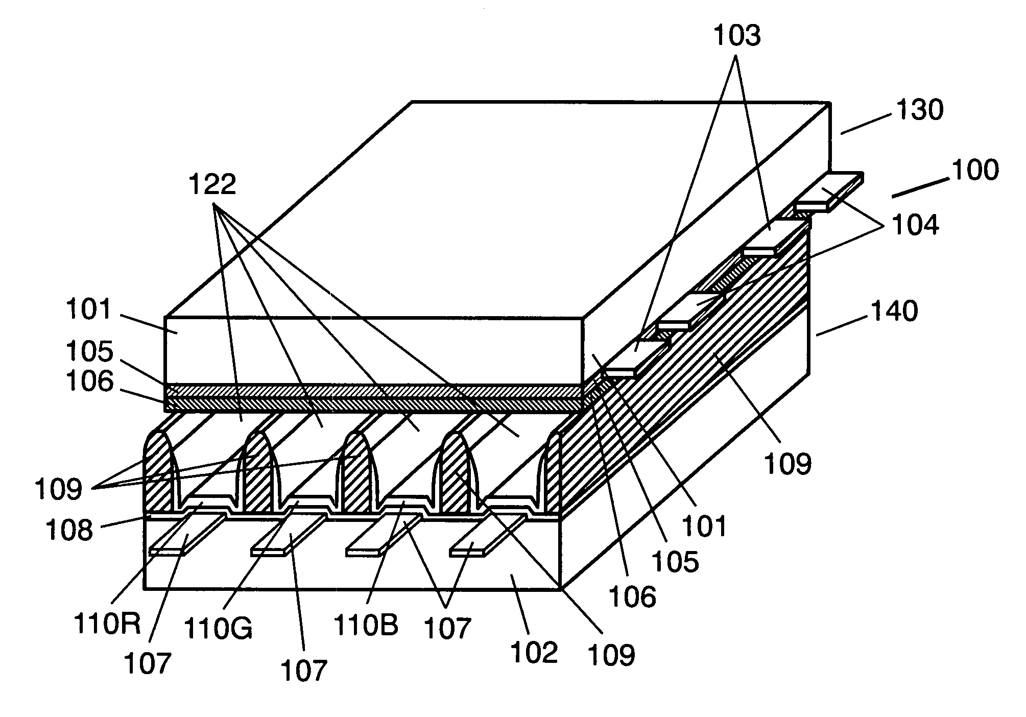
[0022]FIG. 1 is a plan view showing a schematic configuration of electrodes of the PDP. PDP 100 is equipped with a front glass substrate (not shown in the figure), rear glass substrate 102, sustain electrode 103, scan electrode 104, address electrode 107, and airtight seal layer 121. N of each sustain electrodes 103 and each scan electrodes 104 are arranged in parallel to each other. M of address electrodes 107 are arranged in parallel. Sustain electrode 103, scan electrodes 104, and address electrode 107 have an electrode matrix of a three-electrode structure, and a discharge cell is formed at a crossing point of scan electrode 104 and address electrode 107.

[0023]FIG. 2 is a partial cross-section perspective view in an image display region of the PDP. PDP 100 is configured with front panel 130 and rear panel 140. Sustain electrode 103, scan electrode 104, dielectric glass layer 105, and MgO protective layer 106 are formed on front glass substrate 101 of front panel 130. Address ele...


PUM

PropertyMeasurementUnit
thicknessaaaaaaaaaa
thicknessaaaaaaaaaa
temperatureaaaaaaaaaa

Abstract

A plasma display device having a panel main body in which a pair of transparent substrates is arranged in opposition so as to form a discharge space between the substrates on at least a front side, barrier ribs are arranged on at least one of the substrates to divide the discharge space into a plurality of spaces, a group of electrodes is arranged on the substrates so as to generate discharge in the discharge space divided with the barrier ribs, and phosphor layers that emit by discharge are provided, in which the phosphor layers are equipped with a green phosphor layer including at least Zn2SiO4:Mn, a surface of Zn2SiO4:Mn is coated with magnesium oxide, and a ratio of an Mg element to a Si element on the surface measured with an XPS apparatus is 0.7 to 4.0.

Description

[0001]THIS APPLICATION IS A U.S. NATIONAL PHASE APPLICATION OF PCT INTERNATIONAL APPLICATION PCT / JP2007 / 053083.BACKGROUND OF THE INVENTION[0002]I. Technical Field[0003]The present invention relates to a plasma display device and a method of manufacturing a phosphor material constituting a phosphor layer thereof.[0004]II. Description of Related Art[0005]A plasma display device (below, written as “a PDP device”) has attracted attention as an image display device capable of realizing high definition and a large screen in recent years.[0006]A plasma display panel (below, written as “PDP”) is a part where the images of the PDP device are displayed, and is configured with a front substrate and a rear substrate. The front substrate is configured with display electrodes consisting of a striped transparent electrode and a metal bus electrode formed on a glass substrate, a dielectric layer covering the display electrodes, and a protective layer. On the other hand, the rear substrate is config...

Claims


Application Information

Patent Timeline
Patent Type & Authority Patents(United States)
IPC IPC(8): H01J17/49C09K11/54C09K11/08C09K11/59H01J11/22H01J11/24H01J11/34H01J11/42
CPCC09K11/595H01J11/12H01J11/42C09K11/54C09K11/59C09K11/57
Inventor NAGASAKI, YOSHIHISATOYODA, IZUMIHIBINO, JUNICHISUGIMOTO, KAZUHIKOHORIKAWA, KEIJISHIGETOH, NOBUYUKIMIYAMAE, YUICHIRO
Owner PANASONIC CORP