Device mounting board and semiconductor apparatus using the same

a technology of device mounting and semiconductor, applied in the direction of printed circuit, non-metallic protective coating application, printed element electric connection formation, etc., can solve the problem of deteriorating position accuracy, affecting the effect of positioning accuracy, and requiring high-level miniaturization of the package itsel

Inactive Publication Date: 2011-10-18
SANYO ELECTRIC CO LTD
View PDF13 Cites 0 Cited by
  • Summary
  • Abstract
  • Description
  • Claims
  • Application Information

AI Technical Summary

Benefits of technology

[0010]The present invention has been achieved in view of the foregoing circumstances. It is thus an object of the present invention to stably provide a device mounting board which has a reduced thickness and size, has high reliability and heat resistance, and allows excellent position accuracy in mounting a semiconductor device.
[0012]The cardo type polymer has excellent mechanical strength, heat resistance, and a low coefficient of thermal expansion since its bulky substituents hinder movement of the main chain. This suppresses a drop in adhesiveness between the individual insulating layers in the laminated film of the device mounting board, exfoliation of the layers, or the like ascribable to heat cycles. It is therefore possible to stably provide a device mounting board of high reliability and heat resistance.
[0013]Since the insulating layer containing the cardo type polymer has the thickness smaller than that of the insulating layer arranged between the insulating layer containing the cardo type polymer and the substrate, it is possible to reduce the thickness and size of the device mounting board. The insulating layer containing the cardo type polymer has excellent insulation and exposure performance, high rigidity, and a low coefficient of thermal expansion. The insulating layer, even if thinner than the insulating layer arranged closer to the substrate, can thus fix the entire device mounting board and suppress warpage of the entire device mounting board. This makes it possible to provide a device mounting board that allows excellent position accuracy in mounting a semiconductor device.

Problems solved by technology

Consequently, while the LSI chips of higher integration have grown in the numbers of I / Os, miniaturization has been highly required of the packages themselves.
As a result, there can occur a drop in adhesiveness between the insulating resin layers of the multilayer insulating film, or exfoliation of the layers.
In other cases, the device mounting board can cause warpage, which might deteriorate the position accuracy and cause a drop in yield when semiconductor devices are connected by such connection methods as flip-chip and wire-bonding.
It has thus been difficult to reduce the thicknesses and sizes of the device mounting boards.

Method used


Image

  • Device mounting board and semiconductor apparatus using the same
  • Device mounting board and semiconductor apparatus using the same
  • Device mounting board and semiconductor apparatus using the same

Examples


embodiment 1

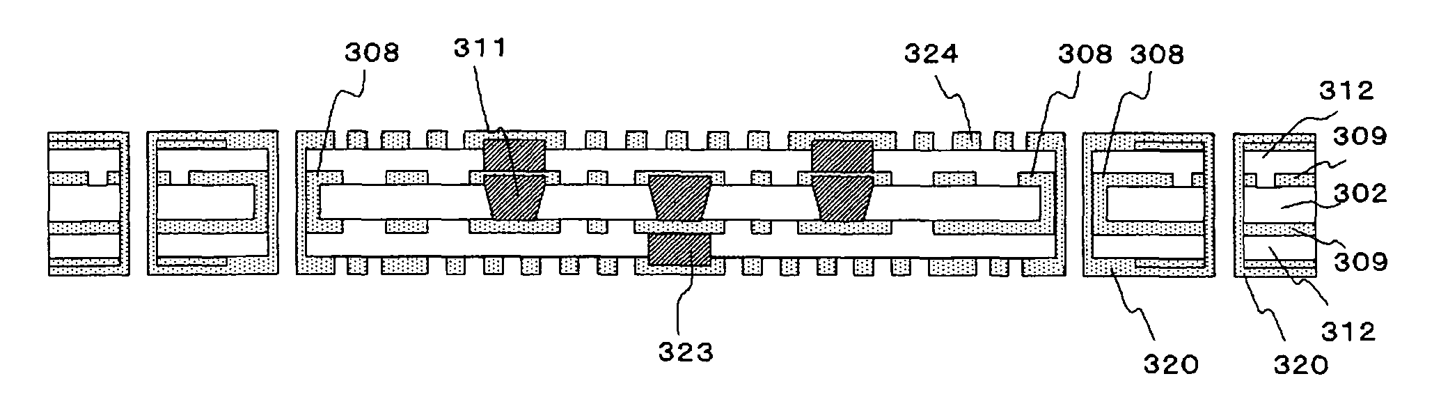
[0059]FIG. 10B is a sectional view showing a device mounting board having a four-layer ISB structure according to the present embodiment. The device mounting board according to the present embodiment is configured so that an insulating resin film 312 and a photosolder resist layer 328 are laminated in this order on the top surface of a substrate 302. Moreover, an insulating resin film 312 and a photosolder resist layer 328 are also laminated in this order on the bottom surface of the substrate 302.

[0060]The substrate 302, the insulating resin films 312, and the photosolder resist layers 328 are pierced by through holes 126.

[0061]Wiring made of a copper film 308, wiring made of a copper film 320, vias 311, and the like are partly embedded in the substrate 302. The wiring made of the copper film 308, the wiring made of the copper film 320, the vias 311, vias 323, and the like are partly embedded in the insulating resin films 312. The wiring made of the copper film 320, the vias 323, a...

embodiment 2

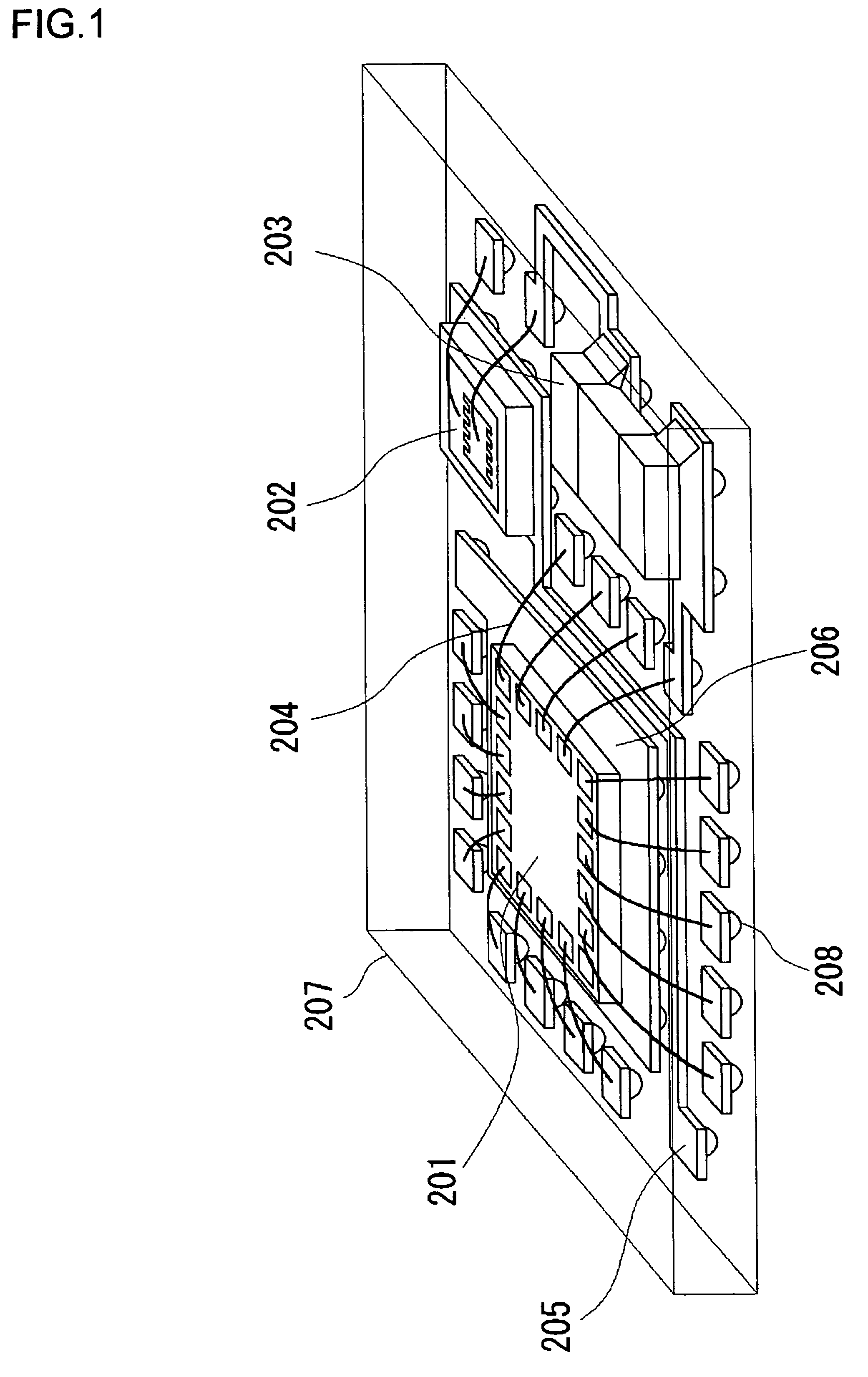
[0150]FIGS. 13A to 13D are sectional views schematically showing various types of semiconductor apparatuses which are formed by mounting a semiconductor device(s) on the semiconductor mounting board described in the embodiment 1.

[0151]There are various modes of semiconductor apparatuses having a semiconductor device(s) mounted on the device mounting board described in the foregoing embodiment 1. For example, in some modes, semiconductor devices are mounted by flip-chip connection or wire-bonding connection. In some modes, semiconductor devices are mounted on the device mounting board in a face-up structure or a face-down structure. In some modes, semiconductor devices are mounted on either one or both of the sides of the device mounting board. Moreover, these various modes may be combined.

[0152]Specifically, for example, a semiconductor device 500 such as an LSI may be mounted on the top of the device mounting board 400 of the embodiment 1 in a flip-chip fashion as shown in FIG. 13A...


PUM


Abstract

A device mounting board for a device to be mounted on, comprising: a substrate; and a laminated film composed of a plurality of insulating layers formed on one side of the substrate. Here, any of the second and subsequent insulating layers from the substrate is a photosolder resist layer containing a cardo type polymer. The photosolder resist layer has a thickness smaller than that of the insulating resin film arranged between the photosolder resist layer and the substrate.

Description

BACKGROUND OF THE INVENTION[0001]1. Field of the Invention[0002]The invention relates to a device mounting board and a semiconductor apparatus using the same.[0003]2. Description of the Related Art[0004]Portable electronics equipment including cellular phones, PDAs, DVCs, and DSCs has been advancing at increasingly fast speed. Under the circumstances, miniaturization and weight saving have become essential in order for these products to be accepted in the market. For the sake of achieving this, system LSIs of higher integration have been sought after. Meanwhile, enhanced usability and convenience have been desired of such electronics equipment, and functional and performance sophistication has been required of the LSIs to be used for the equipment. Consequently, while the LSI chips of higher integration have grown in the numbers of I / Os, miniaturization has been highly required of the packages themselves. For the sake of satisfying both the requirements, there has been a strong dema...

Claims


Application Information

Patent Timeline
Patent Type & Authority Patents(United States)
IPC IPC(8): H01L23/48H01L23/12H01L23/14H05K3/28H05K3/40H05K3/46
CPCH01L23/145H05K3/287H05K3/4655H05K3/4069H05K3/4652H05K2201/0191H01L2224/45144H01L2924/3025H01L2224/48227H01L2224/16225H01L2924/00014H01L2924/00H01L2924/181H01L2924/00012
Inventor USUI, RYOSUKENAKAMURA, TAKESHI
Owner SANYO ELECTRIC CO LTD
Why Eureka
Try Eureka