Method for cutting protective tape of semiconductor wafer and apparatus for cutting the protective tape

a technology of protective tape and semiconductor wafer, which is applied in the direction of metal working equipment, metal-working machine components, manufacturing tools, etc., can solve the problems of uneven finished state of the cut end of the tape, high facility cost, and high facility cost, and achieve excellent accuracy and precision

Inactive Publication Date: 2011-10-25
NITTO DENKO CORP
View PDF9 Cites 3 Cited by
  • Summary
  • Abstract
  • Description
  • Claims
  • Application Information

AI Technical Summary

Benefits of technology

[0012]The present invention has been accomplished taking such actual circumstances into consideration. That is, the present invention aims at providing a method for cutting a protective tape of a semiconductor wafer allowing cutting process of the tape having excellent accuracy and precision by a stable contact pressure of a cutter blade pushed against a periphery of a wafer, from the start to end of cutting process, in a process for cutting a protective tape by a rotating travel of a cutter blade, and also aims at providing an apparatus for cutting the protective tape.
[0014]automatically controlling the pushing biasing force corresponding to the variation of the traveling speed of the cutter blade, to allow stable maintenance for the contact pressure of the cutter blade to the outer circumferential edge of the semiconductor wafer.
[0015]According to the method for cutting the protective tape of the semiconductor wafer of the present invention, when the cutter blade is in a condition in contact with the outer circumferential edge of the wafer at a starting position of cutting, a predetermined contact pressure is applied on the cutter blade caused by a pushing biasing force. Start of the rotating travel of the cutter blade generates a centrifugal force applying to the cutter blade, and to a component for supporting the cutter blade, responding to the speed. Therefore, this centrifugal force reduces the contact pressure of the cutter blade to the outer circumferential edge based on the centrifugal force. Here, the variation of the contact pressure of cutter blade in a state with a blade halting and in a state with a centrifugal force generated is determined beforehand, and thus the compensation control of the pushing force of the cutter blade is performed, based on this variation. This compensation control enables the maintenance of a constant contact pressure of the cutter blade from the start to end of cutting process, therefore achieving uniform finish of the cut end of the tape all over the wafer peripheries. Furthermore, cutting of the protective tape having reliable agreement of the positions of the start and the end of cutting may be guaranteed.
[0019]In another method, an external force (pushing force) in a direction opposite to the centrifugal force is applied as the cutter blade starts traveling and generates a centrifugal force, allowing stable maintenance of a contact pressure of the cutter blade having a magnitude at the start point of time of cutting.
[0030]The fixed end of the spring is linked with an actuator, and thus the amount of operation of the actuator is controlled based on the traveling speed of the cutter blade detected by a sensor.

Problems solved by technology

In order to cope with such disadvantages, the method needs a motor for rotating and driving the chuck table having a larger force output, and exhibiting a larger starting torque, and simultaneously having a braking mechanism with a higher capability, etc., leading to consequent higher facility costs.
As a result, these factors cause higher facility costs.
However, in the method, the rotative travel of the cutter blade causes possible problems.
As a result, there may arise a problem of uneven finished state of the cut end of the tape in the circumferential direction.

Method used


Image

  • Method for cutting protective tape of semiconductor wafer and apparatus for cutting the protective tape
  • Method for cutting protective tape of semiconductor wafer and apparatus for cutting the protective tape
  • Method for cutting protective tape of semiconductor wafer and apparatus for cutting the protective tape

Examples


Embodiment Construction

[0051]Hereinafter, embodiments of the present invention will be described with reference to drawings.

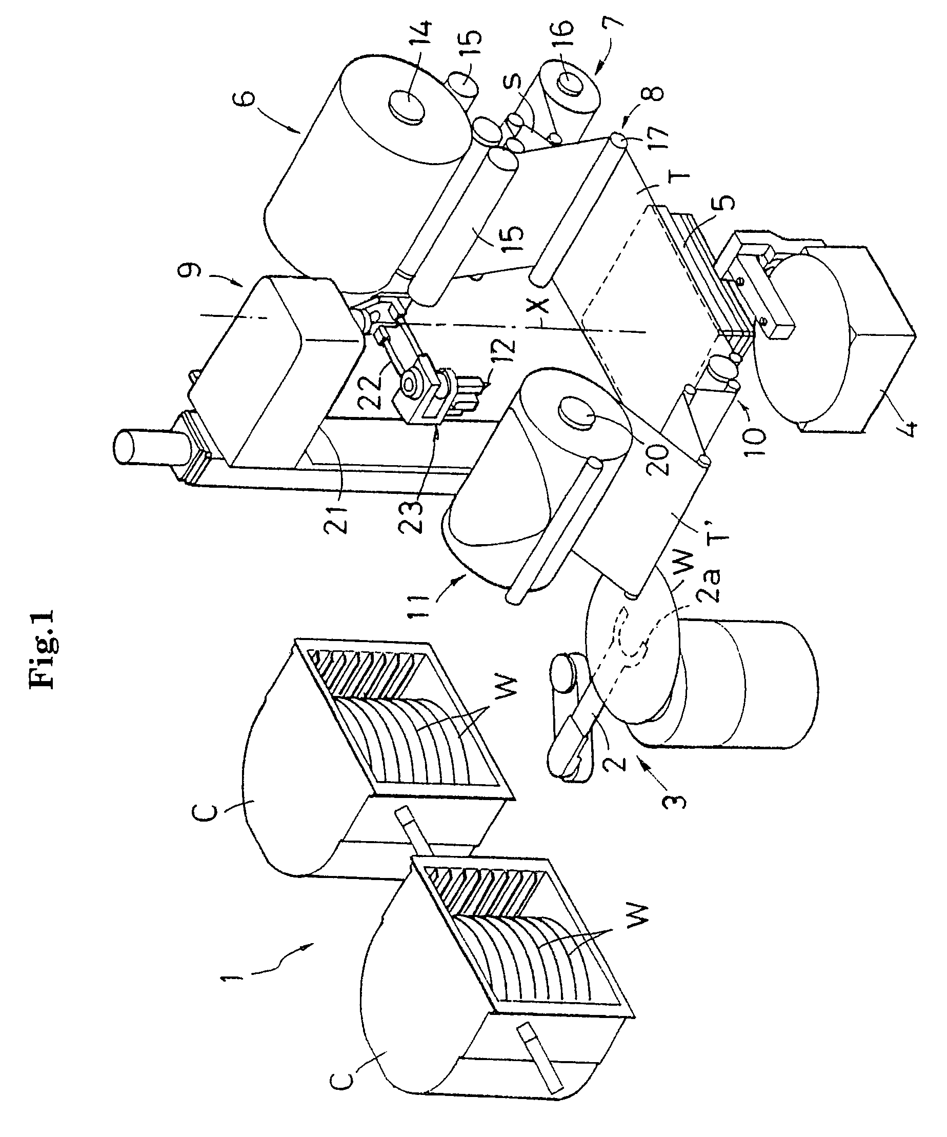
[0052]FIG. 1 is a perspective view illustrating a configuration of a whole apparatus for applying a protective tape.

[0053]As FIG. 1 illustrates, the apparatus for applying a protective tape comprises:

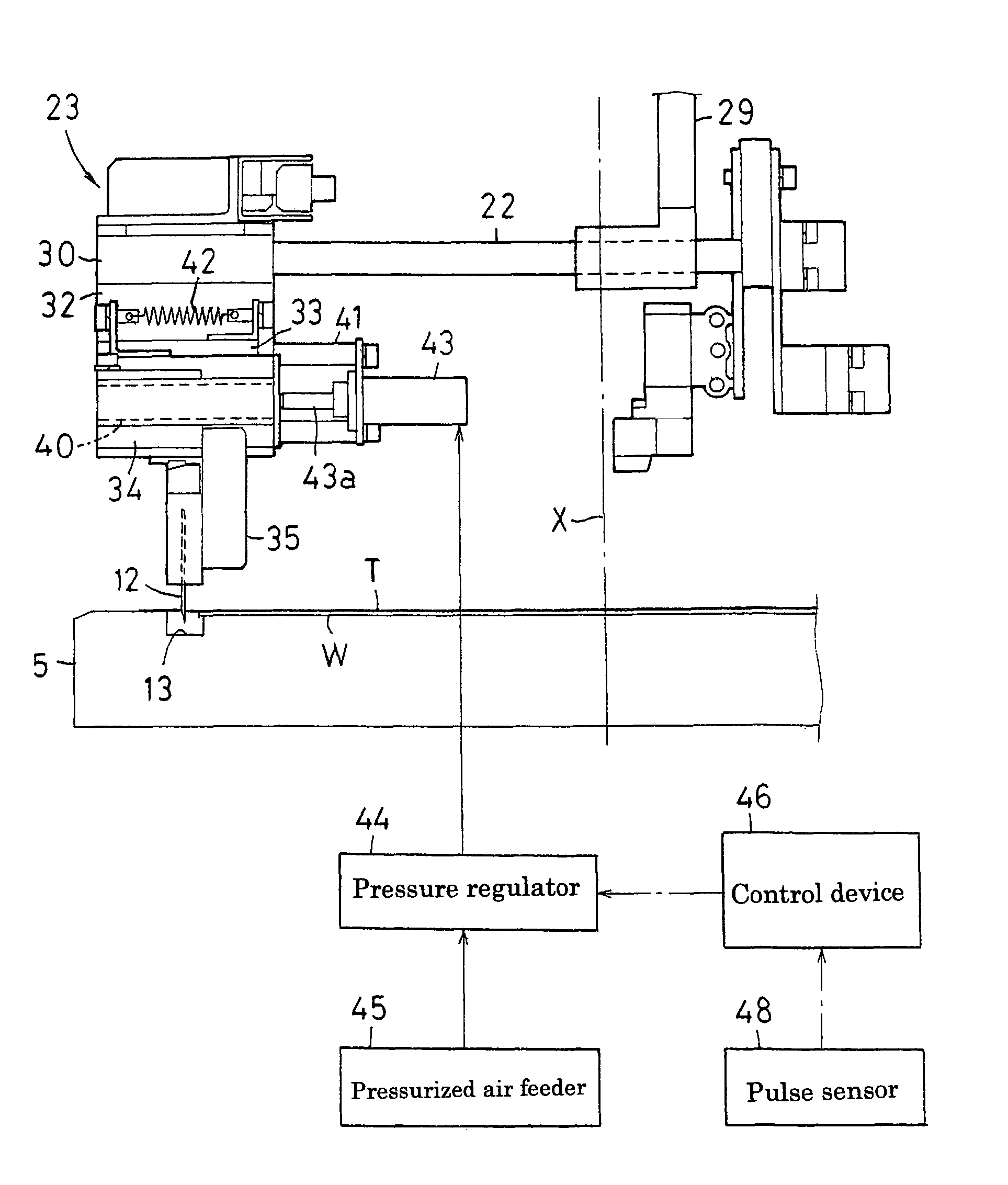
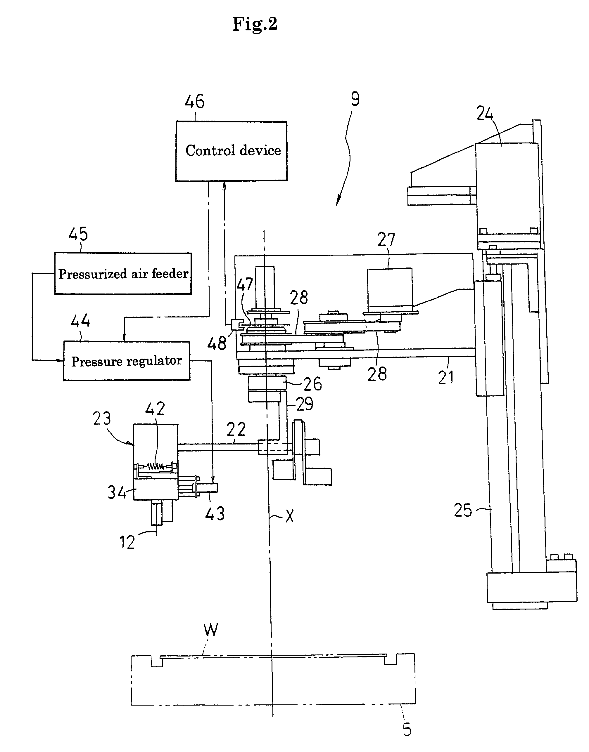
[0054]a wafer feeding / collecting section 1 for loading a cassette C that contains a semiconductor wafer W (hereinafter abbreviated as “wafer” for short); a wafer transport mechanism 3 provided with a robot arm 2; an alignment stage 4; a chuck table 5 for mounting and suction-holding the wafer W; a tape feed section 6 for feeding a protective tape T for surface protection to the wafer W; a separator collecting section 7 for separating and collecting a separator s from the protective tape T with the separator fed from the tape feed section 6; an application unit 8 for applying the protective tape T to the wafer W mounted and suction-held in the chuck table 5; an apparatus 9 for cutting the...


PUM

PropertyMeasurementUnit
elastic restoring forceaaaaaaaaaa
forceaaaaaaaaaa
biasing forceaaaaaaaaaa

Abstract

A cutter blade movably in a radial direction of a wafer is pressed for biasing to an outer circumferential edge of the semiconductor wafer. Simultaneously, the pushing biasing force of the cutter blade is controlled constant with automatic regulation corresponding to a traveling speed variation of the cutter blade, so that effect of a centrifugal force that works at the time of rotating travel of the cutter blade may not vary a pushing biasing force of the cutter blade. As a result, a contact pressure of the cutter blade to the outer circumferential edge of the semiconductor wafer is maintained stable.

Description

BACKGROUND OF THE INVENTION[0001](1) Field of the Invention[0002]The present invention relates to a method for cutting a protective tape applied on the surface of a semiconductor wafer along with the contour of the wafer by traveling a cutter blade along with an outer circumferential edge of the semiconductor wafer, and relates to an apparatus for cutting the protective tape.[0003](2) Description of the Related Art[0004]As methods for cutting protective tapes, there is known a method, wherein a protective tape is supplied and applied on the surface of a semiconductor wafer mounted and maintained on a chuck table; and subsequently the chuck table is rotated with a cutter blade stuck into the protective tape, that is, in the method the cutter blade is configured to travel relatively along with an outer circumferential edge of the wafer so as to cut the protective tape along with the contour the of the wafer (refer to JP-A 2004-25402).[0005]As other methods for cutting protective tapes...

Claims


Application Information

Patent Timeline
Patent Type & Authority Patents(United States)
IPC IPC(8): B23Q15/00
CPCB26F1/3846H01L21/67132Y10T83/162Y10T83/8776Y10T83/173Y10T83/141H01L21/48
Inventor KANESHIMA, YASUJINISHINOHAMA, TAKASHIYAMAMOTO, MASAYUKI
Owner NITTO DENKO CORP
Why Eureka
Try Eureka