
Heater, reflow apparatus, and solder bump forming method and apparatus

a technology of reflow apparatus and solder bump, which is applied in the direction of metal-working apparatus, solid-state devices, printed circuit assembling, etc., can solve the problems of insufficient melting of upper solder particles far from the pad electrode, and achieve the reduction of variations in the manufacture of solder bumps, the suppression of oxidation of solder paste or the like on the substrate, and the effect of reducing the size (height) of the solder bump

Inactive Publication Date: 2011-10-25
TAMURA KK +1
View PDF14 Cites 9 Cited by
  • Summary
  • Abstract
  • Description
  • Claims
  • Application Information

AI Technical Summary

Benefits of technology

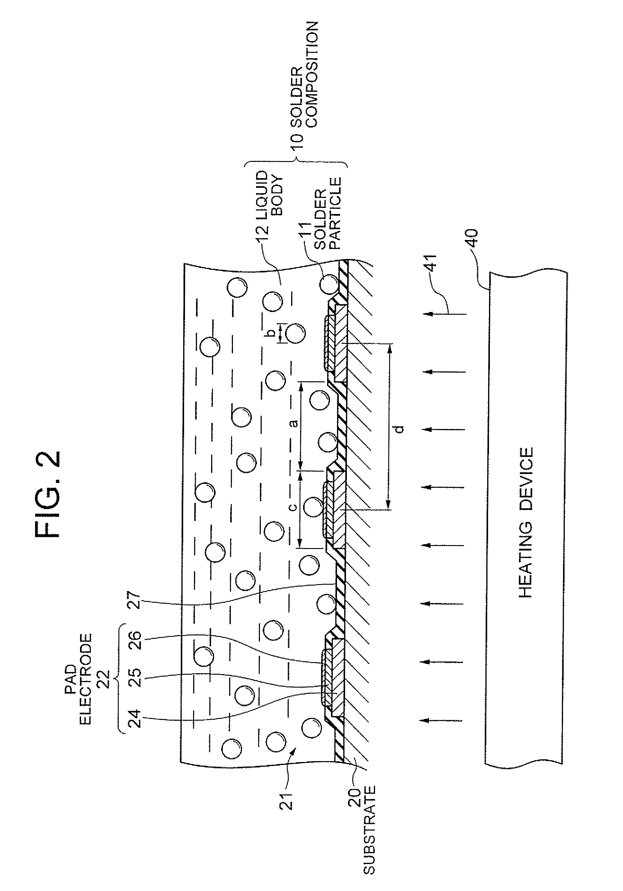
[0014]When the solder composition on the substrate is heated from the substrate side, the temperature of the solder composition becomes lower towards the top-face side and becomes higher towards the substrate side. Thus, the lower solder particles near the pad electrode start to melt first and, when melted, they are wet and spread over the pad electrodes. At that time, the upper solder particles far from the pad electrode have not sufficiently been melted yet. Thus, it is possible to reduce the risk of uniting the solder particles with each other, thereby suppressing generation of solder bridges as well.
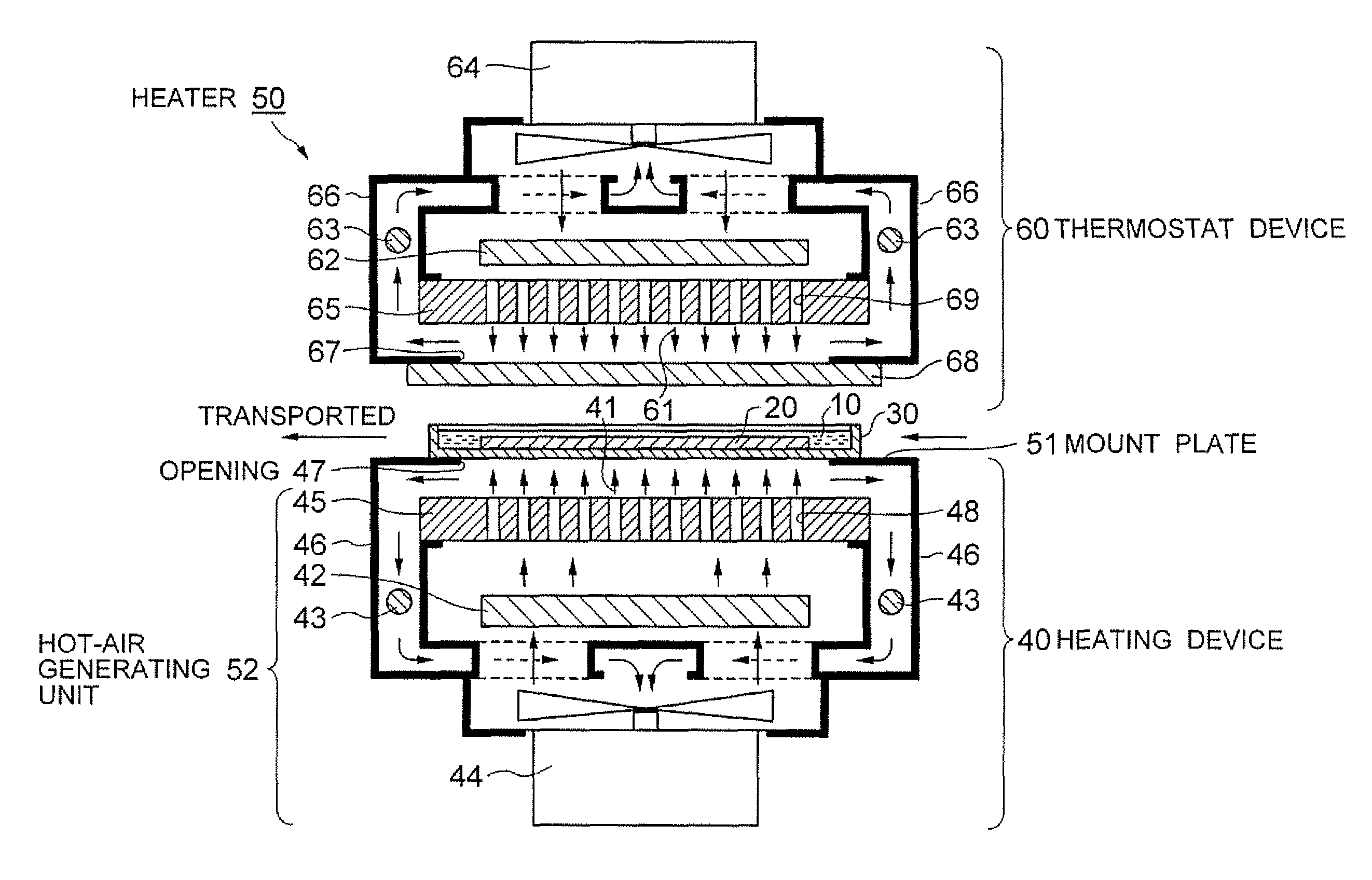
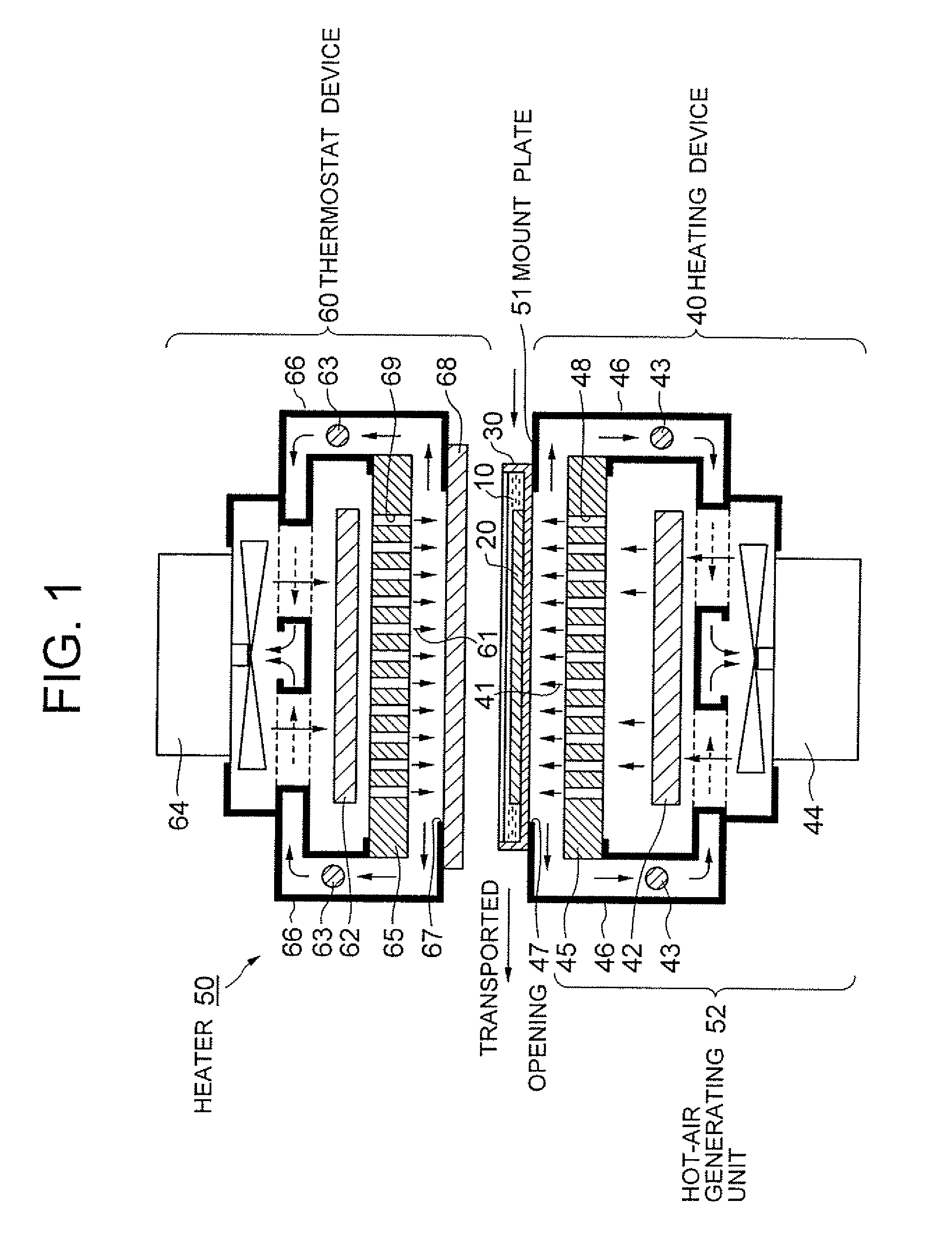
[0062]In the method of using the reflow apparatus according to the present invention, a dummy substrate or the like is fed before, after, or in the middle of a plurality of the substrates or the like, thereby suppressing blow-out of the hot air from the opening when the opening is not covered by the substrate or the like. Moreover, fluctuation of the thermal capacity in terms of the heater is reduced so that fluctuation in the temperature of the hot air can be suppressed.

Problems solved by technology

At that time, the upper solder particles far from the pad electrode have not sufficiently been melted yet.

Method used


Image

  • Heater, reflow apparatus, and solder bump forming method and apparatus
  • Heater, reflow apparatus, and solder bump forming method and apparatus
  • Heater, reflow apparatus, and solder bump forming method and apparatus

Examples


example 1

[0159]EXAMPLE 1 as a more concrete example of this embodiment will be described hereinafter.

[0160]The solder particles used therein had the composition of Sn(96.5 wt %)-Ag(3.0 wt %)-Cu(0.5 wt %) with the melting point at 218° C., and the average diameter thereof was 6 μm (particle size distribution of 2-11 μm). A kind of (trimethylpropanetrioleate) of fatty ester was used for the liquid body. The main characteristic of fatty ester is that the kinematic viscosity at 40° C. is 48.3 mm2 / s, the kinematic viscosity at 100° C. is 9.2 mm2 / s, and the acid value is 2.4. An organic acid was not added and those originally contained in free fatty acid were utilized. Further, vacuum deaeration with less than the vapor pressure of water was performed on the fatty ester for suppressing the influence of moisture as much as possible.

[0161]For the substrate for forming the solder bumps, a silicon chip with 10 mm square was used. On the silicon chip, pad electrodes in 80 μm pitch were formed in a two-...


PUM

PropertyMeasurementUnit
grain diameteraaaaaaaaaa

Abstract

An apparatus characterized by a feature that in a stage on which a substrate or a jig holding a substrate is mounted, an opening closed when the substrate or the jig is mounted is provided and the substrate or the jig is heated by blowing hot air against the lower portion of the substrate or the jig and by a feature that a solder bump is formed on a pad electrode by heating or reflowing a solder composition which is a mixture containing solder particles, a flux component, and a liquid material which is liquid at normal temperature or changing to liquid when heated, and the composition is heated from the substrate side. With the former feature, oxidization of the solder paste on the substrate where no hot air comes and adhesion of particles to the substrate can be prevented, and with the latter feature, solder particles near the pad electrode are melted earlier and wet and spread over the pad electrode, solder particles above and far from the pad electrode are not melted sufficiently, and an effect of reducing the possibility that solder particles join together can be expected.

Description

TECHNICAL FIELD[0001]The present invention relates to a heater that is optimum for heating solder, for example, and a reflow apparatus using the heater. Furthermore, it relates to bump forming method and apparatus which are used when manufacturing FCs (flip chips) and BGAs (ball grid arrays) by forming protruded solder bumps on a semiconductor substrate and interposer substrate, for example.BACKGROUND ART[0002]In a typical conventional forming method of solder bumps, solder paste is applied on pad electrodes of a substrate by screen printing or a dispensing method, and the solder paste is heated for reflow. The solder paste is also referred to as “cream solder”.[0003]Patent Literature 1 discloses an example of the above-described solder paste. The solder paste depicted in Patent Literature 1 is obtained by forming an oxide film on the surfaces of solder particles by making the solder particles flow in the air. It is noted that the oxide film formed forcibly functions to suppress coa...

Claims


Application Information

Patent Timeline
Patent Type & Authority Patents(United States)
IPC IPC(8): B23K31/02B23K1/012B23K3/06F27B17/00F27D7/02H01L21/48H01L21/60H01L23/12H05K3/34
CPCB23K1/0016B23K1/012B23K3/0623B23K3/08F27B17/0025H01L24/11H01L24/12B23K2201/42H01L21/4853H01L2224/13099H01L2924/01004H01L2924/01013H01L2924/01029H01L2924/0103H01L2924/01033H01L2924/01047H01L2924/01057H01L2924/01078H01L2924/01079H01L2924/01082H01L2924/3025H05K3/3436H05K3/3494H01L2924/01005H01L2924/01006H01L2924/01019H01L2924/01023H01L2924/014H01L2224/1131H01L2924/10253H01L2924/00H01L2224/05022H01L2224/05026H01L2224/05568H01L2224/05001H01L2224/05124H01L2224/05147H01L2224/05155H01L2224/056H01L2224/05624B23K2101/42H01L24/13H01L24/05H01L2224/0401H01L2924/00014H01L2924/01014B23K3/04F27D7/02H01L21/48B23K3/06
Inventor SHIRAI, MASARUONOZAKI, JUNICHISAITO, HIROSHISAKAMOTO, ISAOFURUNO, MASAHIKOANDO, HARUHIKOHIRATSUKA, ATSUSHI
Owner TAMURA KK
Learn More