Fabrication method of two-terminal semiconductor component using trench technology

a two-terminal semiconductor and trench technology, applied in the direction of semiconductor devices, basic electric elements, electrical appliances, etc., can solve the problems of affecting so as to improve the heat dissipation of semiconductor components, reduce the series resistance, and improve the component properties

Active Publication Date: 2011-11-01
DONGGUK UNIV IND ACADEMIC COOPERATION FOUND
View PDF1 Cites 0 Cited by
  • Summary
  • Abstract
  • Description
  • Claims
  • Application Information

AI Technical Summary

Benefits of technology

[0012]Exemplary embodiments may provide a method of fabricating a two-terminal semiconductor component by using a trench technique that uses an etching method to lap and polish a semiconductor substrate for the improvement of the component properties through the reduction of series resistance and the improvement of heat dissipation of the semiconductor component.
[0013]Exemplary embodiments also may provide a method of fabricating a two-terminal semiconductor component that minimizes the deviation in thickness in a lapping and polishing process of a semiconductor substrate and has high reproducibility of a wafer polishing process for a thinner substrate and high uniformity in thickness for the wafer.

Problems solved by technology

These diodes may generate a lot of heat in the materials during the operation, and the generated heat may deteriorate the properties of the components.
However, when the substrate is thinner, it is impossible to fabricate a component on the substrate, and thus GaAs or InP substrates require the thickness of 600 μm or greater for the diameter of 3 inches or greater.
Moreover, it is not technically easy to consistently repeat the fabrication of a semiconductor component with the thickness of 50 μm or less within a minimal error range.

Method used


Image

  • Fabrication method of two-terminal semiconductor component using trench technology
  • Fabrication method of two-terminal semiconductor component using trench technology
  • Fabrication method of two-terminal semiconductor component using trench technology

Examples


Embodiment Construction

[0024]The features and advantages of this invention will become apparent through the below drawings and description.

[0025]A method of fabricating a two-terminal semiconductor component using a trench technique according to a certain embodiment of the present invention will be described below in more detail with reference to the accompanying drawings. This, however, is by no means to restrict the present invention to this embodiment, and shall be construed as including all permutations, equivalents and substitutes covered by the spirit and scope of the present invention. This embodiment presented in the description is intended to implement the present invention and to show those of ordinary skill in the art the scope of the present invention only.

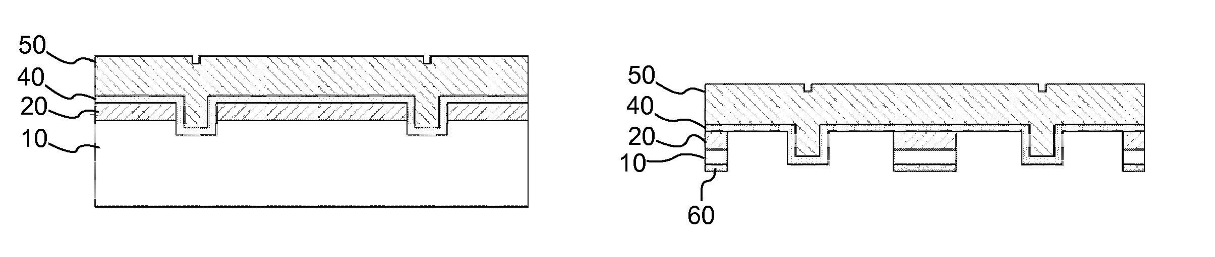
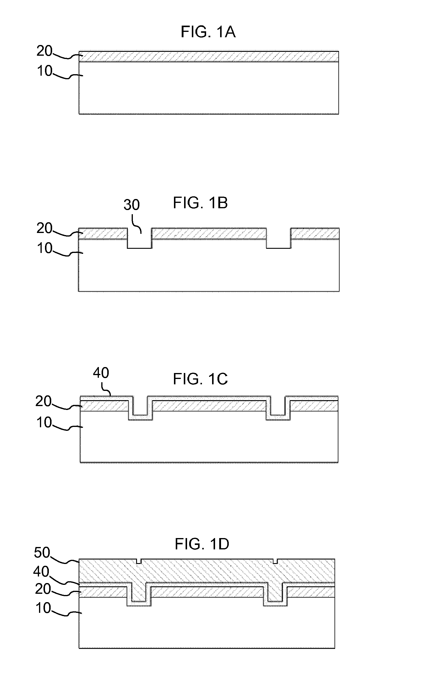
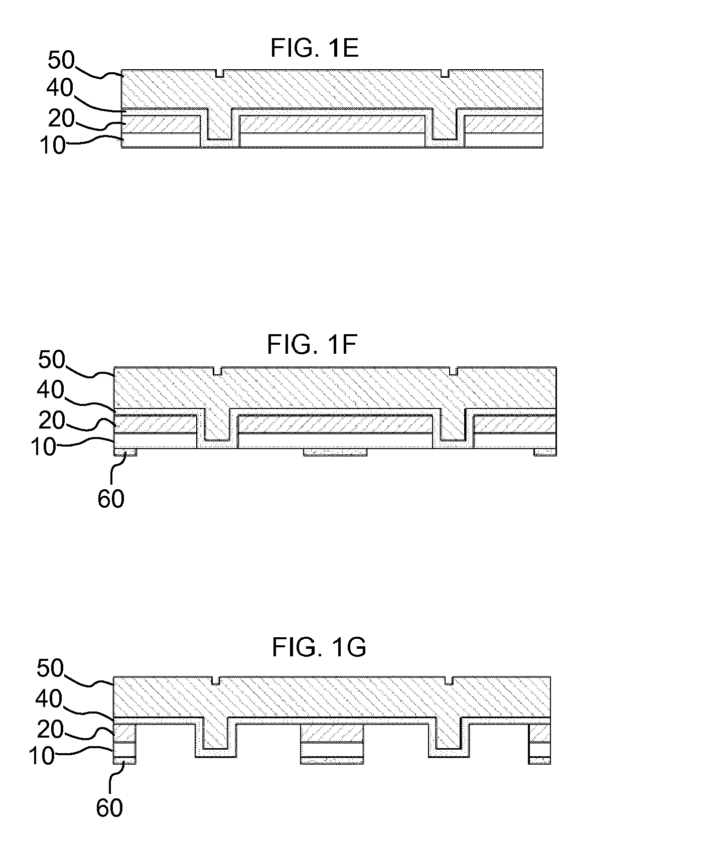
[0026]FIGS. 1A to 1G illustrate the flow of fabricating a two-terminal semiconductor component according to an embodiment of the present invention.

[0027]Referring to FIG. 1A, an active layer 20 with an appropriate amount of impurities is gro...


PUM

PropertyMeasurementUnit
thicknessaaaaaaaaaa
thicknessaaaaaaaaaa
thicknessaaaaaaaaaa

Abstract

A method of fabricating a two-terminal semiconductor component using a trench technique is disclosed that includes forming a trench by etching an etching pattern formed on a substrate on which an active layer having impurities added is grown, forming a front metal layer on a front upper surface of the substrate by using an evaporation method or a sputtering method after removing the etching pattern, forming a metal plated layer on the front surface of the substrate on which the front metal layer is formed, polishing a lower surface of the substrate by using at least one of a mechanical polishing method and a chemical polishing method until the front metal layer is exposed, forming a rear metal layer on the polished substrate, and removing each component by using at least one of a dry etching method and a wet etching method.

Description

CROSS-REFERENCE TO RELATED APPLICATIONS[0001]This application claims the benefit of Korean Patent Application No. 10-2008-0105029, filed with the Korean Intellectual Property Office on Oct. 24, 2008, the disclosure of which is incorporated herein by reference in its entirety.BACKGROUND[0002]1. Technical Field[0003]The following description relates to a method of fabricating a two-terminal semiconductor component that consists of two electrodes, more specifically to a method of fabricating a semiconductor component having two terminals that can minimize the deviation in thickness during the polishing process of a semiconductor substrate and have higher reproducibility of a thinner substrate than the polishing process.[0004]2. Description of the Related Art[0005]Two-terminal electronic components that can be fabricated using a semiconductor include diodes, resistors, capacitors, inductors and the like. Among these, the diode is the most common active component and is employed in vario...

Claims


Application Information

Patent Timeline
Patent Type & Authority Patents(United States)
IPC IPC(8): H01L21/44H01L21/311
CPCH01L21/30625H01L29/66083H01L29/6609H01L29/66166H01L29/66174H01L21/302H01L21/304
Inventor RHEE, JIN-KOOLEE, SEONG-DAEKIM, MI-RAMIN, DAE-HONGKIM, WAN-JOO
Owner DONGGUK UNIV IND ACADEMIC COOPERATION FOUND
Why Eureka
Try Eureka