Insulated gate bipolar transistor (IGBT) electrostatic discharge (ESD) protection devices

a protection device and bipolar transistor technology, applied in semiconductor devices, circuit arrangements, electrical apparatus, etc., can solve the problems of reducing the ability of esd protection devices to be uniformly turned, affecting the catch-up effect, and reducing the heat dissipation ability of ultra-hv devices, so as to improve the esd protection capability

Active Publication Date: 2011-11-01
VANGUARD INTERNATIONAL SEMICONDUCTOR CORPORATION
View PDF7 Cites 5 Cited by
  • Summary
  • Abstract
  • Description
  • Claims
  • Application Information

AI Technical Summary

Benefits of technology

[0006]Accordingly, in order to overcome the problems mentioned previously and to achieve using an insulated gate bipolar transistor (IGBT) device as an electrostatic discharge (ESD) protection device, the drain region layout of IGBT devices has been improved, such that ESD protection devices can be turned on more uniformly to improve ESD protection capability.

Problems solved by technology

For a device experiencing high voltage electrostatic discharge (ESD), an inner circuit may either be damaged or result in a latch-up effect due to an overly high trigger voltage and an overly low holding voltage.
However, by using the silicon-on-insulator (SOT) substrate and fabrication processes thereof, heat dissipation ability of the ultra-HV devices may be diminished.
Meanwhile, during fabrication of high-voltage devices, the diffused concentration of well doped regions is quite low, such that relative impedance increases, therefore, diminishing the ability for the ESD protection devices to be uniformly turned on.

Method used


Image

  • Insulated gate bipolar transistor (IGBT) electrostatic discharge (ESD) protection devices
  • Insulated gate bipolar transistor (IGBT) electrostatic discharge (ESD) protection devices
  • Insulated gate bipolar transistor (IGBT) electrostatic discharge (ESD) protection devices

Examples


Embodiment Construction

[0022]It is to be understood that the following disclosure provides many different embodiments, or examples, for implementing different features of various embodiments. Specific examples of components and arrangements are described below to simplify the present disclosure. These are merely examples and are not intended to be limiting. In addition, the present disclosure may repeat reference numerals and / or letters in the various examples. This repetition is for the purpose of simplicity and clarity and does not in itself indicate a relationship between the various embodiments and / or configurations discussed. Moreover, the formation of a first feature over or on a second feature in the description that follows may include embodiments in which the first and second features are formed in direct contact or not in direct contact.

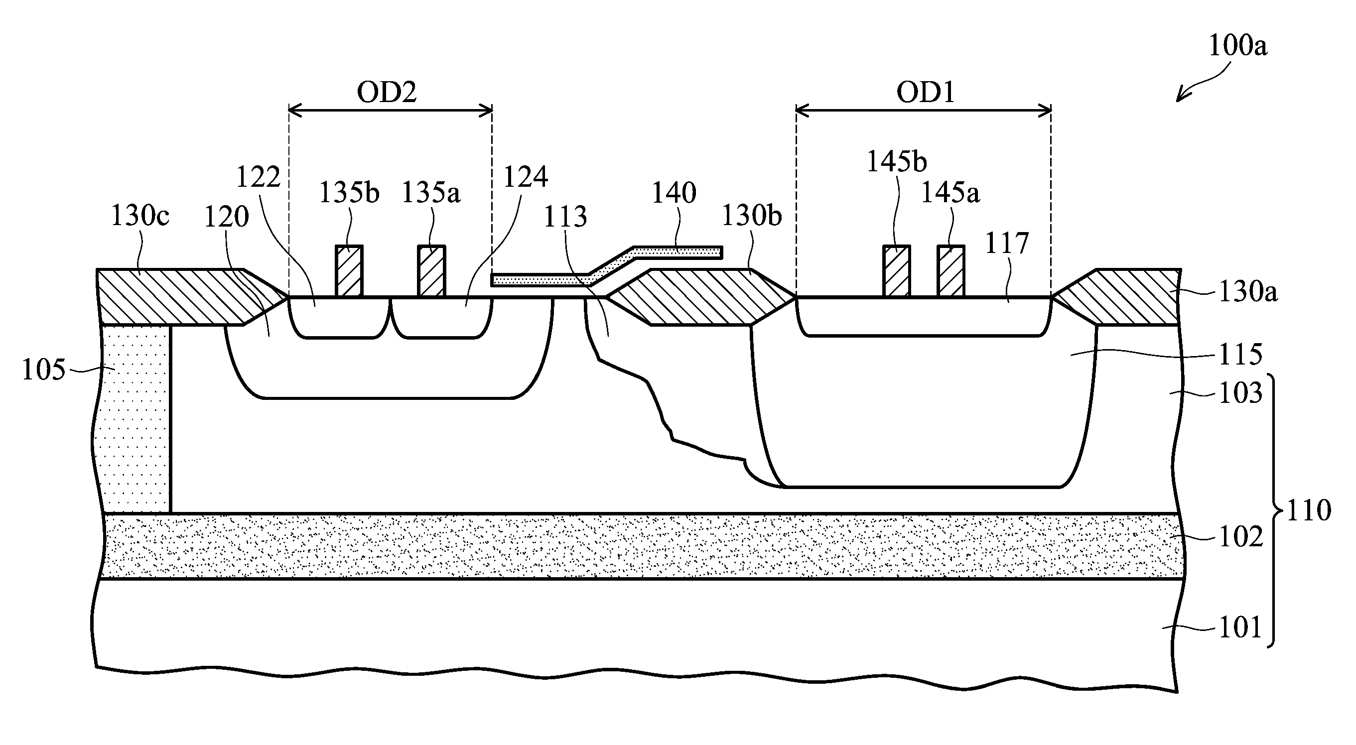
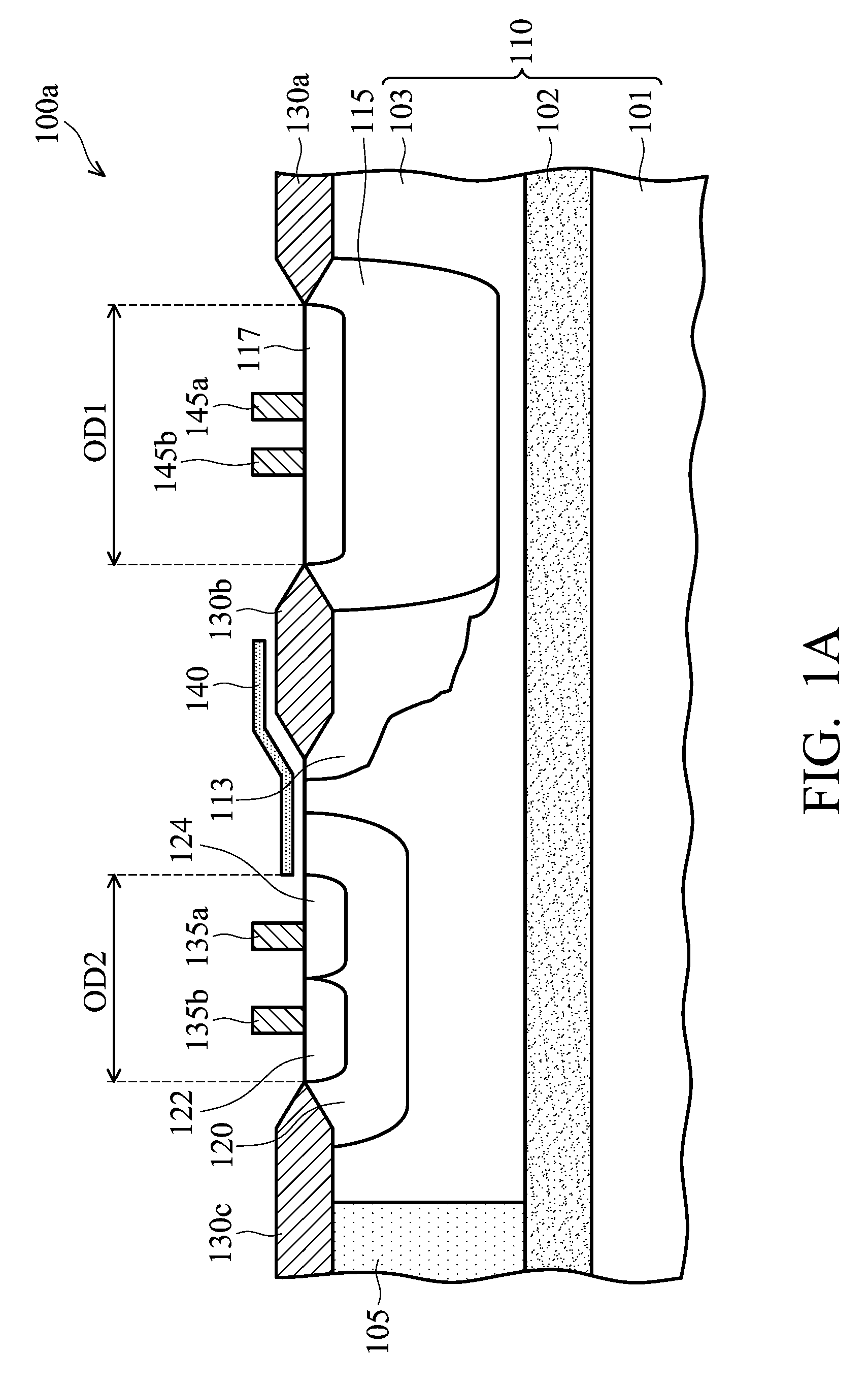
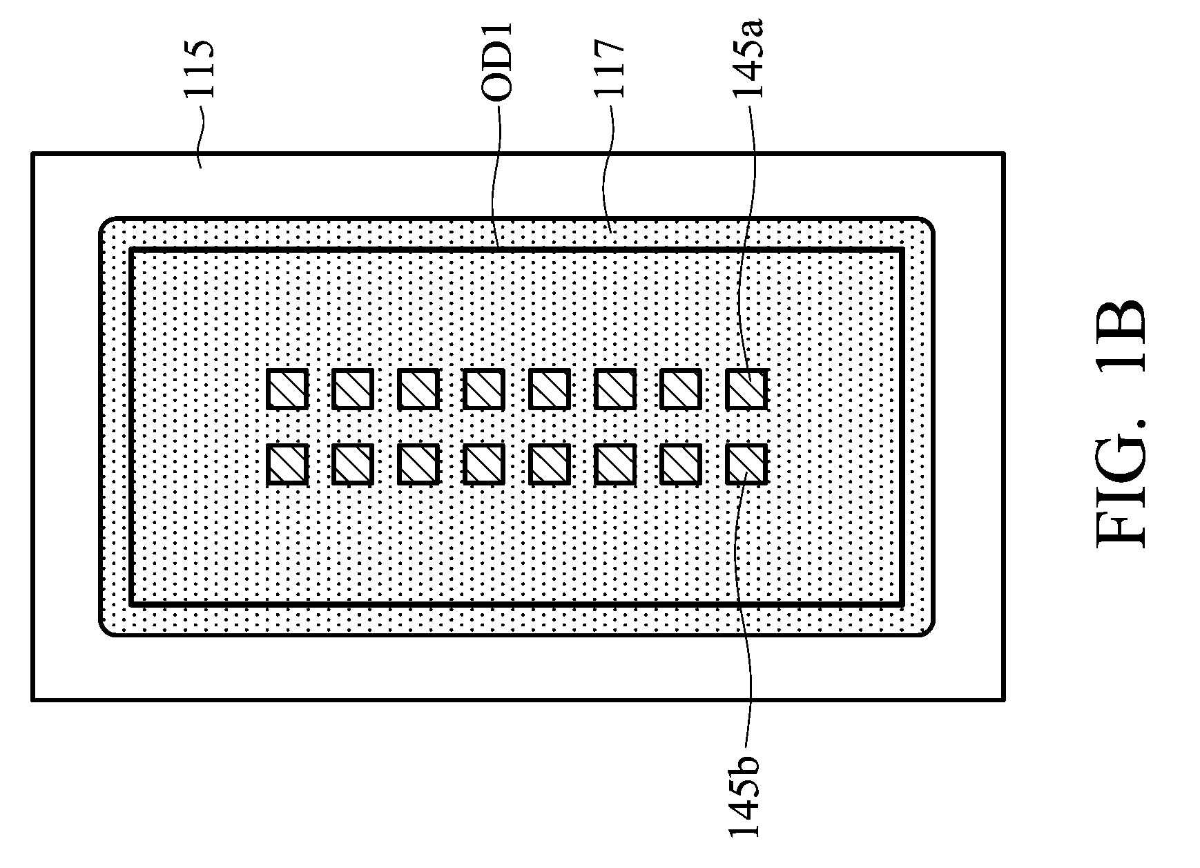
[0023]FIG. 1A is a cross section of an embodiment of the insulated gate bipolar transistor electrostatic discharge (IDBT-ESD) protection device of the invention....


PUM


Abstract

Insulated gate bipolar transistor (IGBT) electrostatic discharge (ESD) protection devices are presented. An IGBT-ESD device includes a semiconductor substrate and patterned insulation regions disposed on the semiconductor substrate defining a first active region and a second active region. A high-V N-well is formed in the first active region of the semiconductor substrate. A P-body doped region is formed in the second active region of the semiconductor substrate, wherein the high-V N-well and the P-body doped region are separated with a predetermined distance exposing the semiconductor substrate. A P+ doped drain region is disposed in the high-V N-well. A P+ diffused region and an N+ doped source region are disposed in the P-body doped region. A gate structure is disposed on the semiconductor substrate with one end adjacent to the N+ doped source region and the other end extending over the insulation region.

Description

BACKGROUND OF THE INVENTION[0001]1. Field of the Invention[0002]The invention relates to electrostatic discharge (ESD) protection devices, and in particular, to insulated gate bipolar transistor electrostatic discharge (IGBT-ESD) protection devices.[0003]2. Description of the Related Art[0004]Conventional high voltage electrostatic discharge (ESD) protection devices include lateral diffused metal oxide semiconductor (LDMOS) power transistors, metal oxide semiconductor field effect transistors (MOSFET), silicon control rectifiers (SCR), bipolar junction transistors (BJT), diodes and field oxide devices (FOD). For a device experiencing high voltage electrostatic discharge (ESD), an inner circuit may either be damaged or result in a latch-up effect due to an overly high trigger voltage and an overly low holding voltage. Therefore, by adding an additional driving circuit to the device, or by regulating layout parameters, trigger voltage can be reduced such that a holding voltage of the ...

Claims


Application Information

Patent Timeline
Patent Type & Authority Patents(United States)
IPC IPC(8): H01L29/93
CPCH01L27/0259H01L29/7393
Inventor JOU, YEH-NINGTU, SHANG-HUICHANG, JUI-CHUNWU, CHEN-WEI
Owner VANGUARD INTERNATIONAL SEMICONDUCTOR CORPORATION
Why Eureka
Try Eureka