Memory controller, nonvolatile storage device, nonvolatile storage system, and nonvolatile memory address management method
a memory controller and storage device technology, applied in the direction of memory architecture accessing/allocation, instruments, computing, etc., can solve the problems of reducing the life of the leveling method, reducing the number of times, and requiring an extremely long time period for reading, so as to prolong the life of the nonvolatile storage device and increase the rewriting frequency
- Summary
- Abstract
- Description
- Claims
- Application Information
AI Technical Summary
Benefits of technology
Problems solved by technology
Method used
Image

Examples
first embodiment
1.1 System Configuration
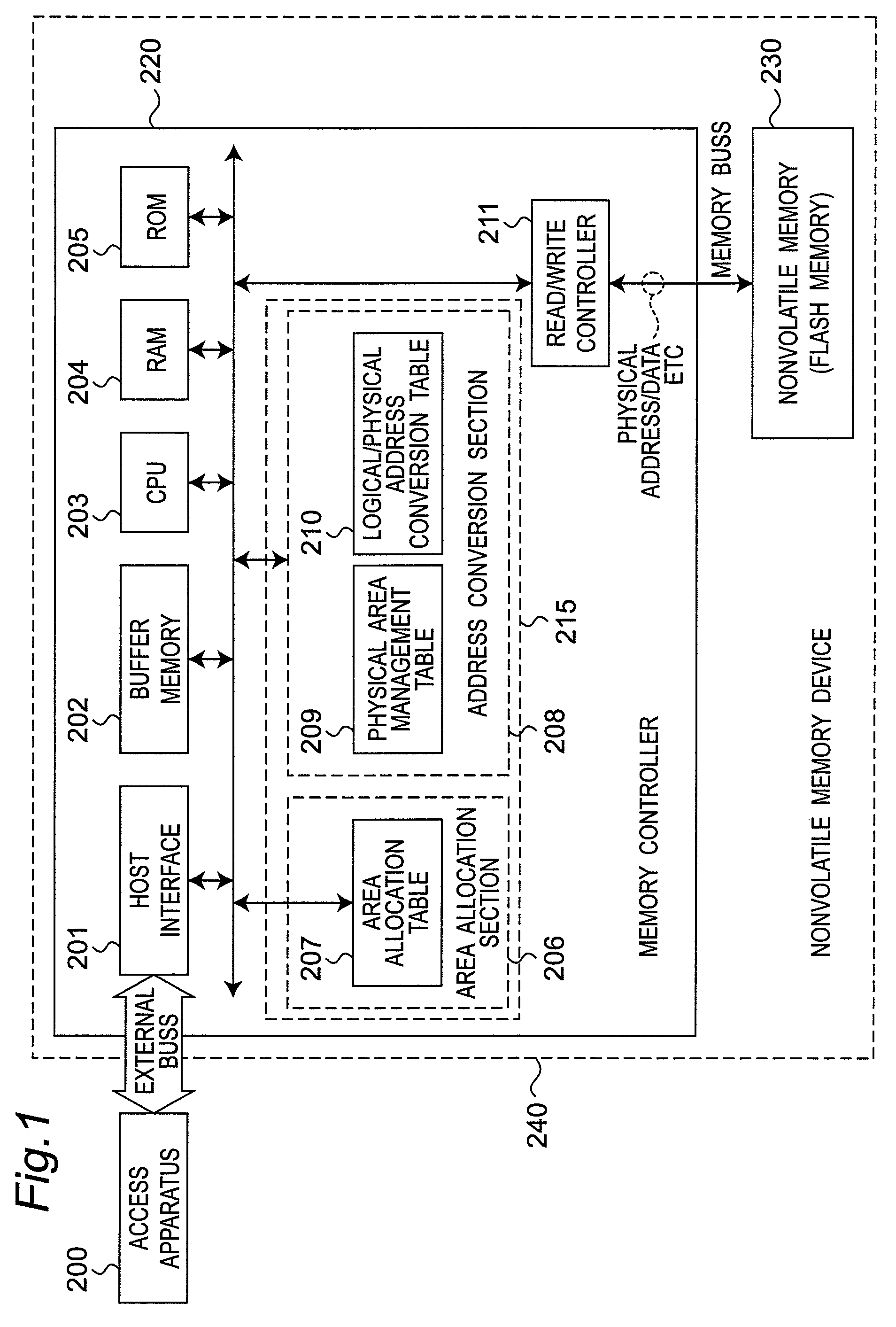
[0059]FIG. 1 is a view illustrating the configuration of a nonvolatile storage system according to a first embodiment of the present invention. The nonvolatile storage system includes an access apparatus 200 and a nonvolatile storage device 240 to and from which data is written and read by the access apparatus 200.
[0060]The nonvolatile storage device 240 stores data therein according to a data writing command from the access apparatus 200 and reads, therefrom, data stored therein according to a data reading command from the access apparatus 200. The nonvolatile storage device 240 includes a memory controller 220 and a nonvolatile memory 230. The memory controller 220 includes a host interface 201, a buffer memory 202, a CPU 203, a RAM 204, a ROM 205, an area allocation section 206, an address conversion section 208, and a read / write controller 211. The area allocation section 206 and the address conversion section 208 constitute an address management section ...
second embodiment
[0116]A nonvolatile system according to the present embodiment is different from that of the first embodiment, in the configuration of the nonvolatile storage device. The configurations and operations of the other portions are the same as those of the first embodiment. Hereinafter, in the present embodiment, there will be described only the configurations and operations different from the first embodiment.
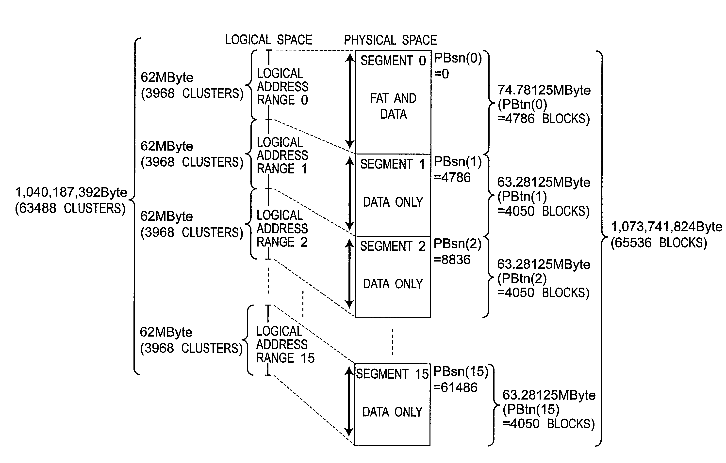
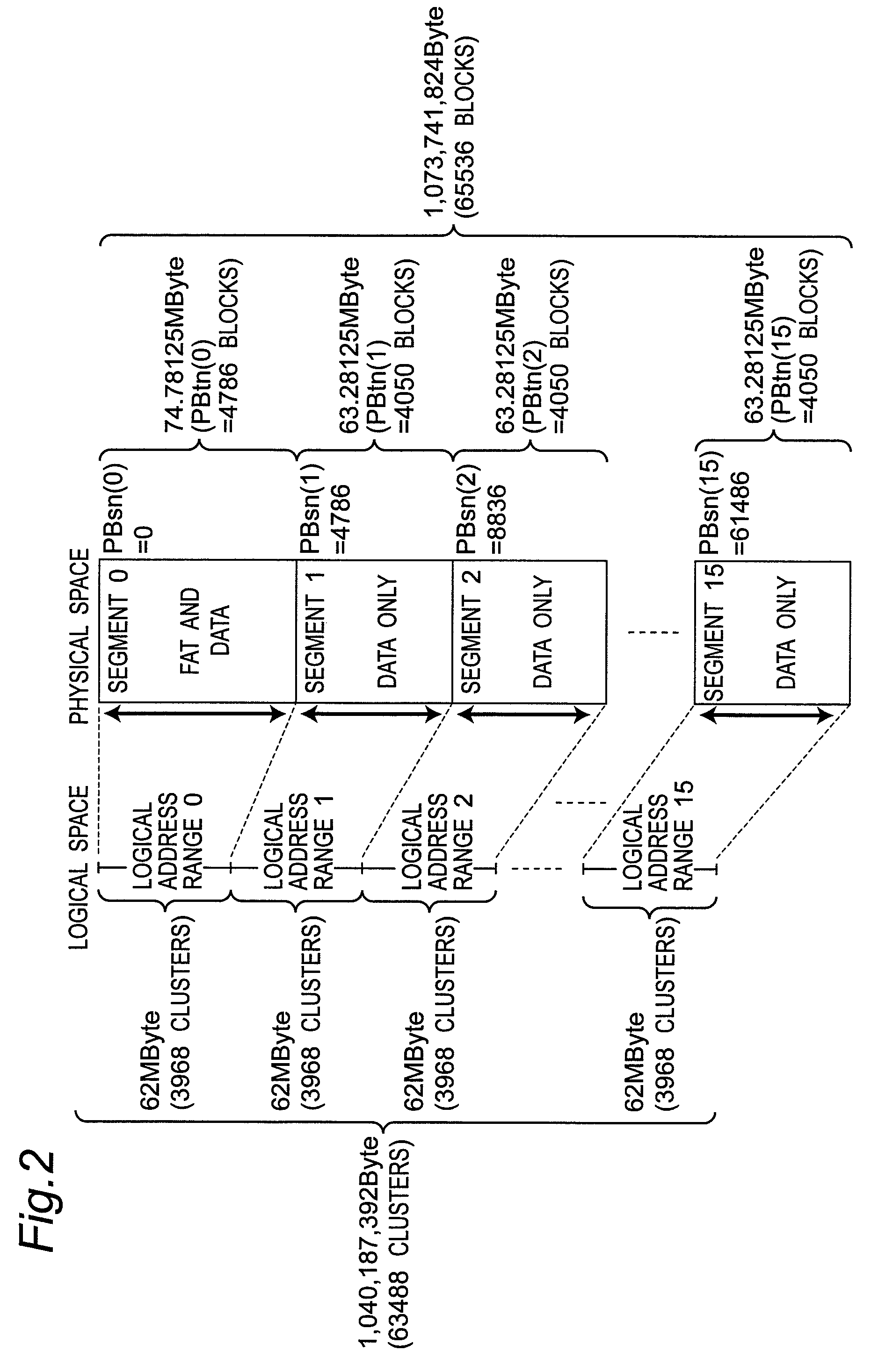
[0117]In the nonvolatile storage device according to the present embodiment, area allocation is determined, such that the logical address range corresponding to a segment having a higher rewriting frequency includes a smaller number of logical blocks, than the numbers of logical blocks included in the other logical address ranges, in order to average the paces at which the respective segments in the physical address ranges reach a guaranteed number of rewritings to extend the life.
2.1 System Configuration
[0118]FIG. 10 is a view illustrating the configuration of a nonvolatile storag...
PUM
 Abstract
Description
Claims
Application Information