Semiconductor laser device

a laser device and semiconductor technology, applied in semiconductor lasers, laser details, electrical equipment, etc., can solve the problems of degrading the characteristics of semiconductor lasers, and reducing the laser performance of lasers

Inactive Publication Date: 2009-06-30
MITSUBISHI ELECTRIC CORP
View PDF12 Cites 235 Cited by
  • Summary
  • Abstract
  • Description
  • Claims
  • Application Information

AI Technical Summary

Benefits of technology

[0016]Thus, the present invention provides an extended life for semiconductor laser device in which an adhesive layer is formed between a coating film and the underlying semiconductor.

Problems solved by technology

(Lower reflectance does not necessarily guarantee higher laser performance.)
However, depending on the coating method used, the facets may be damaged, resulting in degraded characteristics of the semiconductor laser.
In the case of conventional gallium nitride semiconductor lasers, on the other hand, it is known that the coating films tend to delaminate or peel off resulting in degradation of the facet surfaces.
However, metal adhesive layers have low insulating properties (and may cause shorting).
Further, a metal oxide film is difficult to form to a controlled thickness by sputtering.
Further, although a coating film is preferably formed of amorphous or a single crystal, it is difficult to form a hexagonal single crystal.

Method used


Image

  • Semiconductor laser device
  • Semiconductor laser device
  • Semiconductor laser device

Examples


Embodiment Construction

[0021]Preferred embodiments of the present invention will now be described with reference to the accompanying drawings. It should be noted that in the following figures, like numerals will be used to denote like or corresponding components to avoid undue repetition.

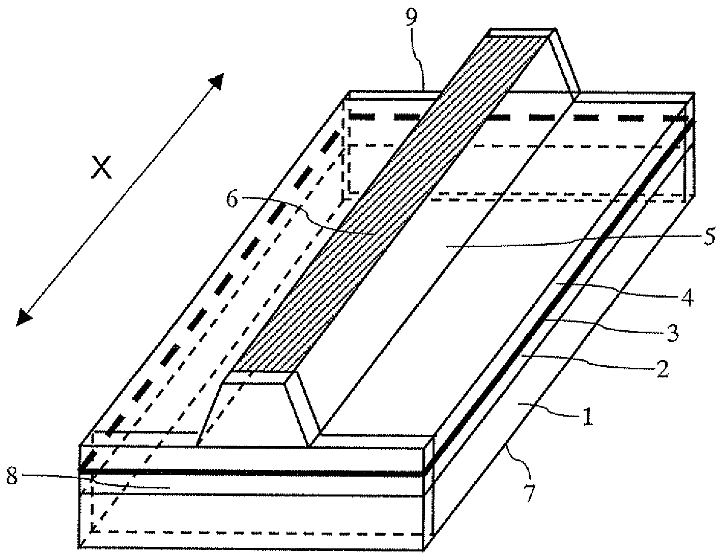
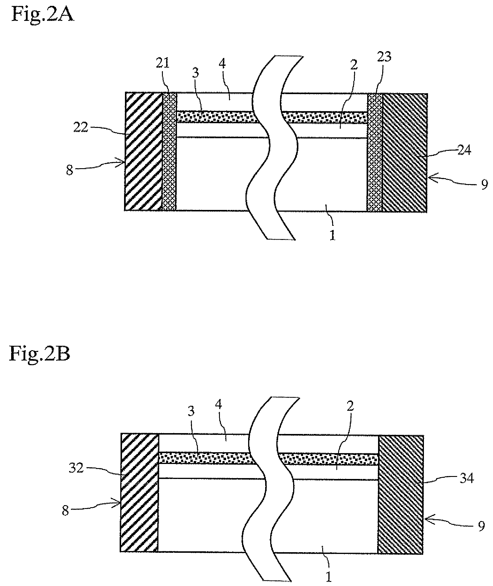
[0022]FIG. 1 is a perspective view of a semiconductor laser device according to an embodiment of the present invention. This semiconductor device is a gallium nitride semiconductor laser device that emits a blue laser beam and employs a GaN substrate 1.

[0023]Referring to FIG. 1, an n-type cladding layer 2, an active layer 3, and a p-type cladding layer 4 are formed on the GaN substrate 1. The p-type cladding layer 4 has portions thereof removed by etching to form a ridge 5. A p-electrode 6 is provided on top of the ridge 5, and an n-electrode 7 is provided on the bottom surface of the GaN substrate 1. A specular surface is provided on each facet of the ridge, and a cavity is formed to extend in the X-direction (as shown i...


PUM


Abstract

A semiconductor laser device includes a cavity extending in a propagation direction of a laser beam (X-direction). A front facet is on one end of the cavity through which the laser beam is emitted. A rear facet is on the other end of the cavity. Further, an adhesive layer and a coating film are on the front facet, and an adhesive layer and a coating film are on the rear facet. The adhesive layers preferably have a thickness of 10 nm or less and preferably include an anodic oxide film of one of Al, Ti, Nb, Zr, Ta, Si, and Hf.

Description

FIELD OF THE INVENTION[0001]The present invention relates to a semiconductor laser device for use in optical disc systems or optical communications, and more particularly to a blue semiconductor laser device formed of gallium nitride semiconductor material.BACKGROUND ART[0002]Semiconductor laser devices have been widely used in optical disc systems and optical communications (see, e.g., Japanese patent publication No. JP-B-3080312, JP-A-2002-100830 and JP-A-2004-296903). These semiconductor laser devices include a cavity to generate a laser beam. The cavity has a front facet formed on one end thereof to emit the laser beam and has a rear facet formed on the other end. An insulating film, or coating film, is formed on each facet to reduce the operating current of the semiconductor laser, to prevent return of light, and to increase the output power.[0003]Generally, in high power semiconductor lasers, a low reflectance coating film is formed on the front facet, and a high reflectance c...

Claims


Application Information

Patent Timeline
Patent Type & Authority Patents(United States)
IPC IPC(8): H01S5/00
CPCB82Y20/00H01S5/028H01S5/22H01S5/34333H01S5/0283H01S5/0287
Inventor YOSHIDA, YASUAKI
Owner MITSUBISHI ELECTRIC CORP
Why Eureka
Try Eureka