Liquid crystal panel and liquid crystal display device

a liquid crystal display and panel technology, applied in liquid crystal compositions, instruments, chemistry apparatus and processes, etc., can solve the problems of slow response and narrow viewing angle of liquid crystal display devices employing tn mode, complex production process, slow response and narrow viewing angle, etc., to achieve wide viewing angle and high contrast

Active Publication Date: 2011-11-08
MERCK PATENT GMBH
View PDF13 Cites 2 Cited by
  • Summary
  • Abstract
  • Description
  • Claims
  • Application Information

AI Technical Summary

Benefits of technology

The present invention is attained in view of the above problems. An object of the present invention is to provide a practical liquid crystal panel and a practical liquid crystal display device each of which is capable of simultaneously achieving characteristics of a high-speed response, a wide viewing angle, and a high contrast.
The liquid crystal panel is driven by a so-called lateral electric field that is parallel to the substrate surface, while a high contrast characteristic due to vertical alignment is maintained. This makes it possible to achieve a wide viewing angle characteristic and a high contrast characteristic by a simple pixel configuration. Moreover, because an initial bend transition operation is unnecessary, practical bend alignment can be achieved.
In the liquid crystal panel, as in a case of an OCB mode, when liquid crystal molecules are to move, liquid crystal molecule flows operate in a direction assisting the movement of the liquid crystal molecules. Therefore, a high-speed response becomes possible. A characteristic of such a high-speed response corresponds to a degree of bend alignment. In the liquid crystal panel, the degree of bend alignment depends on physical properties (in particular Δε·Δn) of the liquid crystal material. However, the degree of bend alignment also varies in accordance with the electrode width and the electrode spacing of the electrodes. By setting the values of the electrode width and the electrode spacing within the above range, it becomes possible to obtain a liquid crystal panel in which a degree of deformation of the liquid crystal alignment is greater than that of a conventional configuration.
In particular, by setting the electrode width of the electrodes to 5 μm or less and the electrode spacing of the electrodes to 15 μm or less, a high transmittance can be obtained by a practical driving voltage. Further, by setting the Δε·Δn to be in a range of 1.3 to 3.1, a high transmittance and a characteristic of a high-speed response can be obtained practically. Therefore, according to the above configuration, it becomes possible to provide a practical liquid crystal panel capable of simultaneously achieving characteristics of (i) a wide viewing angle equivalent to those of an MVA mode and an IPS mode, (ii) a high-speed response as fast as or faster than that of the OCB mode, and (iii) a high contrast.
Therefore, the present invention makes it possible to provide a practical display device capable of simultaneously achieving characteristics of a high-speed response, a wide viewing angle, and a high contrast.

Problems solved by technology

However, a liquid crystal display device employing the TN mode has disadvantages such as a slow response and a narrow viewing angle.
However, the MVA mode liquid crystal display has disadvantages such that (i) a production process is complex and (ii) as with the TN mode liquid crystal display device, a response speed is slow.
However, the IPS mode also has a disadvantage such that a response speed is slow as with the TN mode and the MVA mode.
Further, the IPS mode is not suitable for mobile devices or in-vehicle devices for which a high speed at a low temperature is required.
Therefore, a factor to increase cost is inherent in the OCB mode.
Further, the OCB mode is inferior in a viewing angle characteristic to the MVA mode and IPS mode.
However, the display mode described above has a serious problem such that a driving voltage is high and a light transmittance is low, though having a high contrast and an excellent viewing angle characteristic as described above.
Further, as in the MVA mode, a response characteristic of the display mode is not sufficient for moving image display.
Therefore, this display mode has not been put to practical use yet.
Therefore, there has been no known liquid crystal panel and liquid crystal display device each of which can simultaneously achieve characteristics of a high-speed response, a wide viewing angle, and a high contrast.

Method used


Image

  • Liquid crystal panel and liquid crystal display device
  • Liquid crystal panel and liquid crystal display device
  • Liquid crystal panel and liquid crystal display device

Examples


embodiment 1

One embodiment of the present invention is explained below with reference to FIGS. 1 to 17(b).

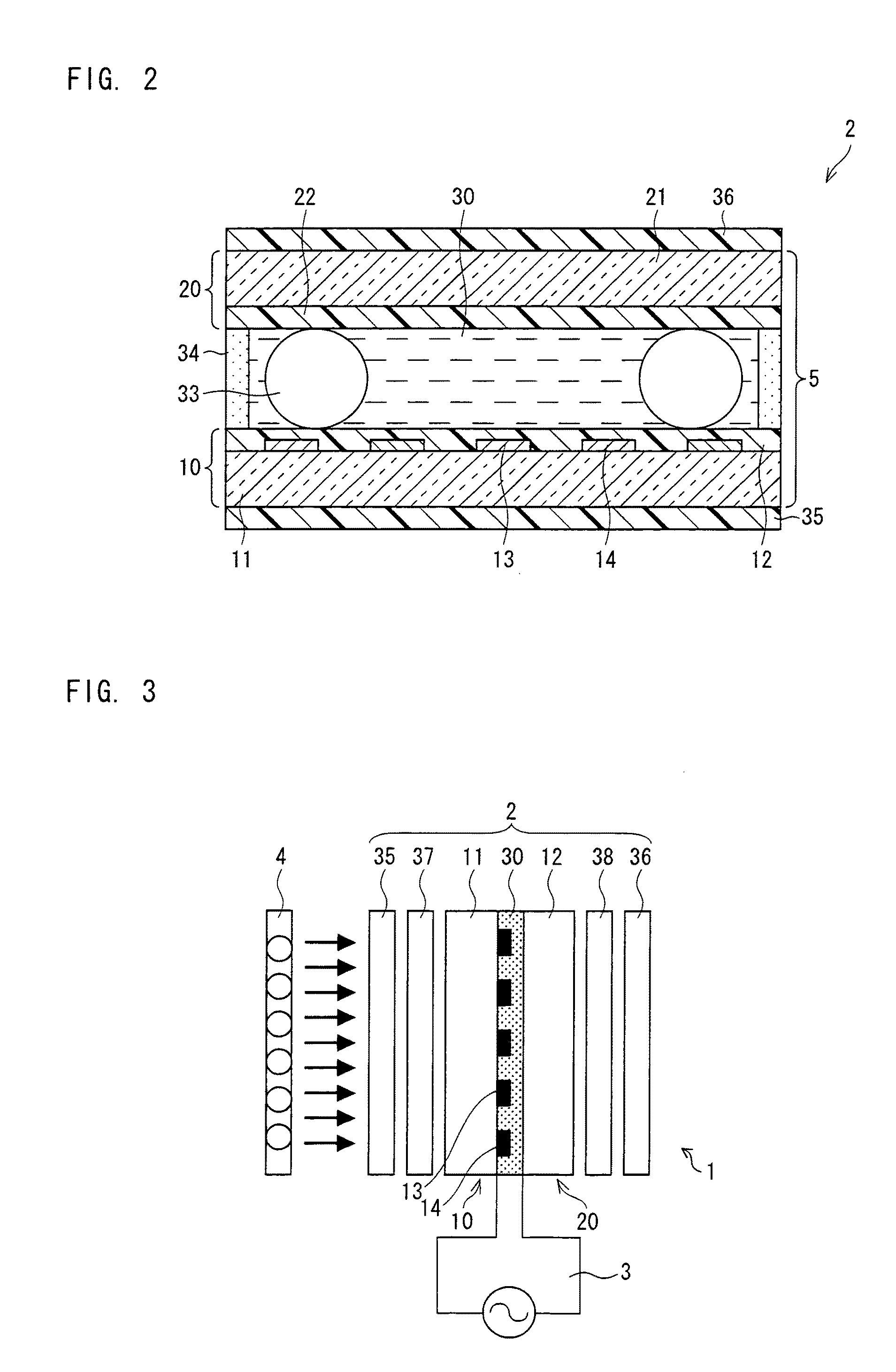
FIG. 3 is an exploded cross sectional view schematically illustrating an outline configuration of a liquid crystal display device according to the present embodiment.

As illustrated in FIG. 3, a liquid crystal display device 1 of the present embodiment includes a liquid crystal panel 2, a driving circuit 3, and a backlight 4 (illumination device). Configurations of the driving circuit 3 and the backlight 4 are the same as configurations of conventional driving circuit and backlight, and explanations thereof are omitted.

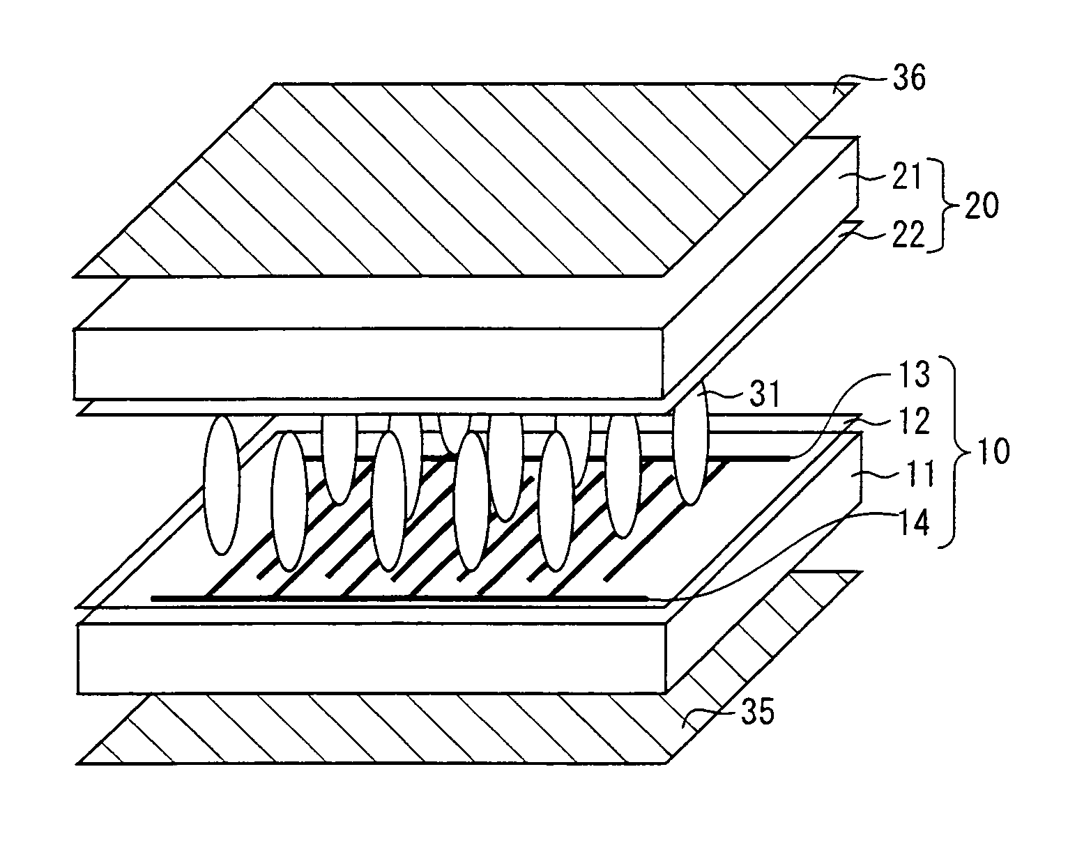
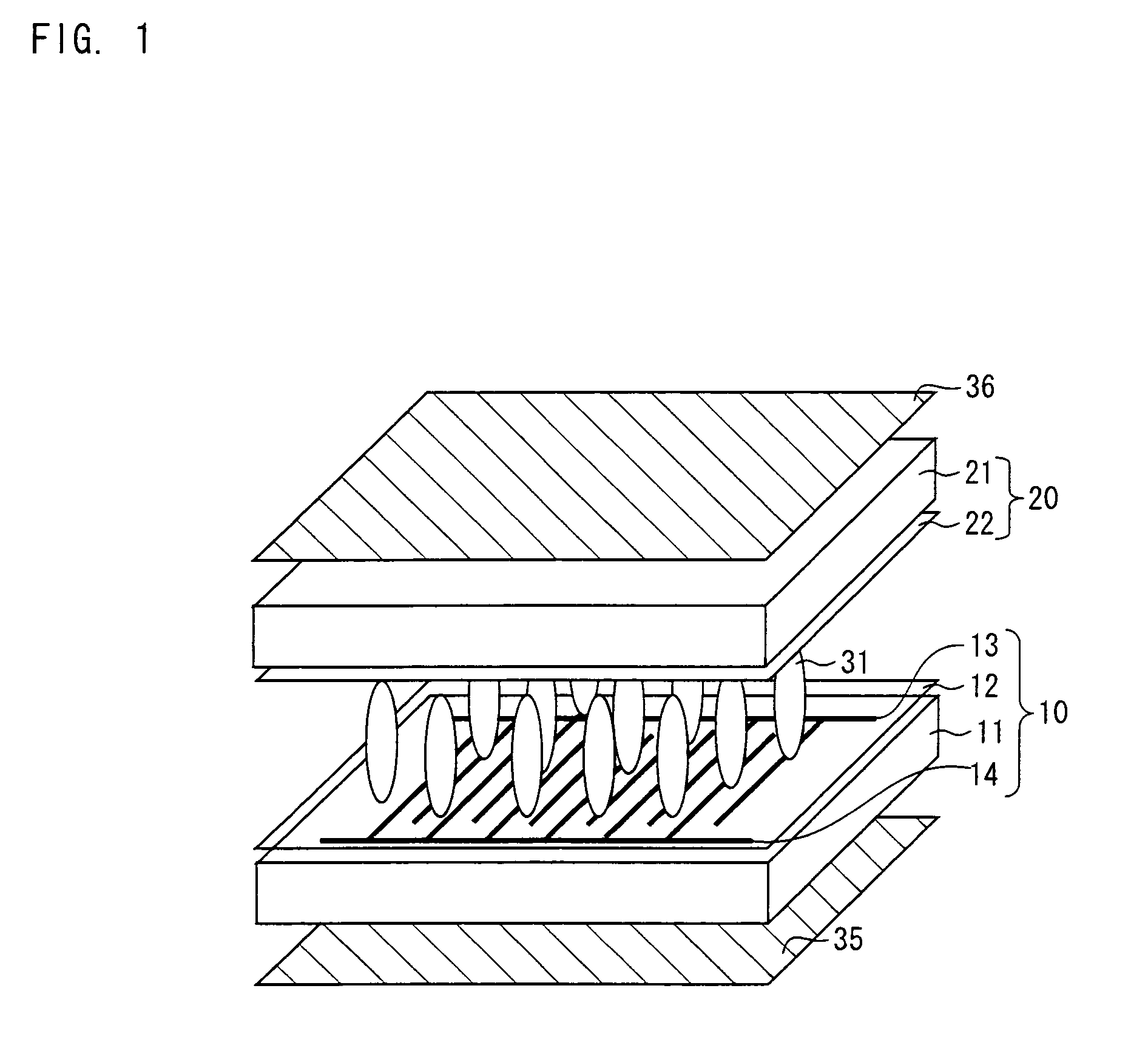
FIGS. 1 and 2 show a typical panel configuration as one example of the liquid crystal panel 2 according to the present embodiment.

FIG. 1 is an exploded perspective view schematically illustrating an outline configuration of a substantial part of the liquid crystal panel 2. FIG. 2 is a cross sectional view schematically illustrating an outline configuration of a substantial par...

example 1

First, an alignment film material “JALS-204” (Product Name, 5% by weight (solid content), γ-butyrolactone solution, produced by JSR Corporation) was applied, by a spin coat method, on a glass substrate that was provided with comb-teeth electrodes 13 and which were made of ITO and that had an electrode width L of 4 μm, an electrode spacing S of 4 μm, and an electrode thickness of 1000 A. Then, the glass substrate with the alignment film material was baked at 200° C. for 2 hours so as to form a substrate 10. A thickness of an alignment film 12 obtained was 600 Å (60 nm).

Next, an alignment film 22 that was identical to the alignment film 12 was formed on a glass substrate 22 so as to form a substrate 20 in the same manner as the substrate 10 except that the comb-teeth shape electrodes 13 and 14 were not provided on the glass substrate 21.

Subsequently, on the substrate 10, resin beads “Micropearl SP” (Product Name, manufactured by Sekisui Chemical Co. Ltd.), as a spacer 33, that had a d...

example 2

Forty liquid crystal panels 2 each having the configuration as shown in FIG. 2 were fabricated in the same manner as Example 1 except that “MLC-6269-000” (Product Name, manufactured by Merck Ltd., p-type nematic liquid crystal material, Δε=17.7 and Δn=0.0984) was used as the liquid crystal material and the electrode width L, the electrode spacing S, and the cell gap d were variously changed.

Next, at 25° C., while an applied voltage was varied from 0V to 20V, a voltage-transmittance characteristic of each of the liquid crystal panels 2 was measured. In the measurement, a rectangular wave of 30 Hz was applied and a wavelength of light for measurement was 550 nm. A relation of the electric application direction and the transmission axis directions of the polarizers 35 and 36 at that time was as shown in FIG. 4. Table 1 shows all relations of the electrode width L, the electrode spacing S, and the maximum transmittance Tmax of the liquid crystal panels 2 each having the cell gap d of 4 ...


PUM

PropertyMeasurementUnit
widthaaaaaaaaaa
widthaaaaaaaaaa
thicknessaaaaaaaaaa

Abstract

A liquid crystal panel includes: a p-type liquid crystal material sandwiched by a pair of substrates and comb-teeth shape electrodes for applying, to the p-type liquid crystal material, an electric field parallel to a substrate surface. The p-type liquid crystal material is aligned vertically with respect to the substrate surface at the time when no electric field is applied. The comb-teeth shape electrodes have an electrode width of 5 μm or less, and an electrode spacing of 15 μm or less. A product of a dielectric constant anisotropy Δε and a refractive index anisotropy Δn of the p-type liquid crystal material is 1.3 or more and 3.1 or less.

Description

This Nonprovisional application claims priority under 35 U.S.C. §119(a) on Patent Application No. 2008-159390 filed in Japan on Jun. 18, 2008, International Application No. PCT / JP2009 / 052835 filed on Feb. 19, 2009, and Patent Application No. 2009-131560 filed in Japan on May 29, 2009, and the entire contents of which are hereby incorporated by reference.FIELD OF THE INVENTIONThe present invention relates to a liquid crystal panel and a liquid crystal display device, in particular, to a liquid crystal panel and a liquid crystal display device each controlling transmission of light by causing bend distortion of a liquid crystal layer by voltage application.BACKGROUND OF THE INVENTIONLiquid crystal display devices have a small thickness, a light weight, and a low power consumption as characteristics, and are used in various fields. Display performance of such liquid crystal display devices is drastically improved year by year. As a result, recently the display performance of liquid cry...

Claims


Application Information

Patent Timeline
Patent Type & Authority Patents(United States)
IPC IPC(8): G02F1/1343
CPCC09K19/3003C09K19/3028C09K19/3059C09K19/3068C09K19/322C09K2019/301C09K2019/3019C09K2019/3021G02F1/134363G02F2001/133397G02F2001/133742G02F2001/13712G02F1/133397G02F1/133742G02F1/13712
Inventor ISHIHARA, SHOICHISAKURAI, TAKEHISAKOZAKI, SHUICHI
Owner MERCK PATENT GMBH
Why Eureka
Try Eureka