Method of fabricating transistor for semiconductor device

a technology of semiconductor devices and fabrication methods, applied in the direction of semiconductor devices, electrical equipment, basic electric elements, etc., can solve the problems of the structure of the conventional pmos transistor and the fabrication method, and achieve the effect of preventing a short channel effect and improving the leakage current characteristic of the transistor

Inactive Publication Date: 2011-11-22
SK HYNIX INC
View PDF5 Cites 19 Cited by
  • Summary
  • Abstract
  • Description
  • Claims
  • Application Information

AI Technical Summary

Benefits of technology

[0018]Embodiments of the present invention are directed to providing a method of fabricating a transistor for use in a semiconductor device. In the method, a source / drain region is formed before growth of an epitaxial layer. At this point, by forming the source / drain region in a state that a trench has been formed by etching a substrate, the source / drain region is sufficiently deep, and the overlap between the side of the source / drain region and a gate pattern is reduced, leading to improving a leakage current characteristic of the transistor and preventing a short channel effect.

Problems solved by technology

As semiconductor devices are being highly integrated, one of important issues is to fabricate transistors that can ensure a high current drivability and a short channel margin even at small dimensions.
However, there are the following limitations on the structure of the conventional PMOS transistor and the fabrication method thereof.

Method used


Image

  • Method of fabricating transistor for semiconductor device
  • Method of fabricating transistor for semiconductor device
  • Method of fabricating transistor for semiconductor device

Examples


Embodiment Construction

[0024]Other objects and advantages of the present invention can be understood by the following description, and become apparent with reference to the embodiments of the present invention.

[0025]Referring to the drawings, the illustrated thickness of layers and regions are exemplary only and may not be exact. When a first layer is referred to as being “on” a second layer or “on” a substrate, it could mean that the first layer is formed directly on the second layer or the substrate, or it could also mean that a third layer may exist between the first layer and the substrate. Furthermore, the same or like reference numerals represent the same or like constituent elements, although they appear in different embodiments or drawings of the present invention.

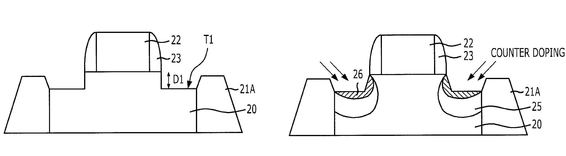
[0026]FIGS. 2A to 2H are cross-sectional views describing a method of fabricating a transistor in accordance with an embodiment of the present invention. In particular, a method of fabricating a PMOS transistor using epitaxial growth is ...


PUM


Abstract

A method of fabricating a transistor in a semiconductor device includes forming a gate structure over a substrate, forming a first trench by etching the substrate on either side of the gate structure to a first depth, ion-implanting dopants of a first conductivity type to form a source / drain region in the substrate on the side of the gate structure with the first trench, etching the substrate on the side of the gate structure with the first trench to a second depth larger than the first depth to form a second trench, and growing an epitaxial layer within the second trench.

Description

CROSS-REFERENCE TO RELATED APPLICATIONS[0001]The present invention claims priority of Korean patent application number 10-2008-0135584, filed on Dec. 29, 2008, the disclosure of which is incorporated herein by reference in its entirety.BACKGROUND OF THE INVENTION[0002]The present invention relates to a semiconductor fabrication technology, and more particularly, to a method of fabricating a transistor for use in a semiconductor device.[0003]As semiconductor devices are being highly integrated, one of important issues is to fabricate transistors that can ensure a high current drivability and a short channel margin even at small dimensions.[0004]Recently, extensive studies have been conducted to increase carrier mobility in order to ensure a high current drivability. Carrier mobility may be increased by applying a certain stress to a channel region defined under a gate, leading to improving current characteristic of transistors. To this end, various transistor structures and fabricati...

Claims


Application Information

Patent Timeline
Patent Type & Authority Patents(United States)
IPC IPC(8): H01L21/336
CPCH01L21/26586H01L29/6656H01L29/66636H01L29/7834H01L29/7848
Inventor SHIN, MIN-JUNG
Owner SK HYNIX INC
Why Eureka
Try Eureka