
Broadband high impedance pickoff circuit

a pickoff circuit and high impedance technology, applied in waveguide type devices, line-transmission details, instruments, etc., can solve problems such as interference, unwanted oscillation and ringing, etc., to dampen parasitic capacitance and minimize parasitic effects of lumped circuit elements

Inactive Publication Date: 2011-11-22
UT BATTELLE LLC
View PDF14 Cites 3 Cited by
  • Summary
  • Abstract
  • Description
  • Claims
  • Application Information

AI Technical Summary

Benefits of technology

The system effectively minimizes parasitic effects, achieving improved high-frequency responses and lower loading, with reduced magnitude and phase distortion, and is safe from electro-static discharge and over-voltage conditions, enabling precise measurement of large voltage ranges without significant signal loss.

Problems solved by technology

Parasitic elements may affect inputs and outputs by reducing bandwidth or by creating unwanted oscillations and ringing.
Measurement systems that display voltage across or current passing through these components may add interference.

Method used


Image

  • Broadband high impedance pickoff circuit
  • Broadband high impedance pickoff circuit
  • Broadband high impedance pickoff circuit

Examples


Embodiment Construction

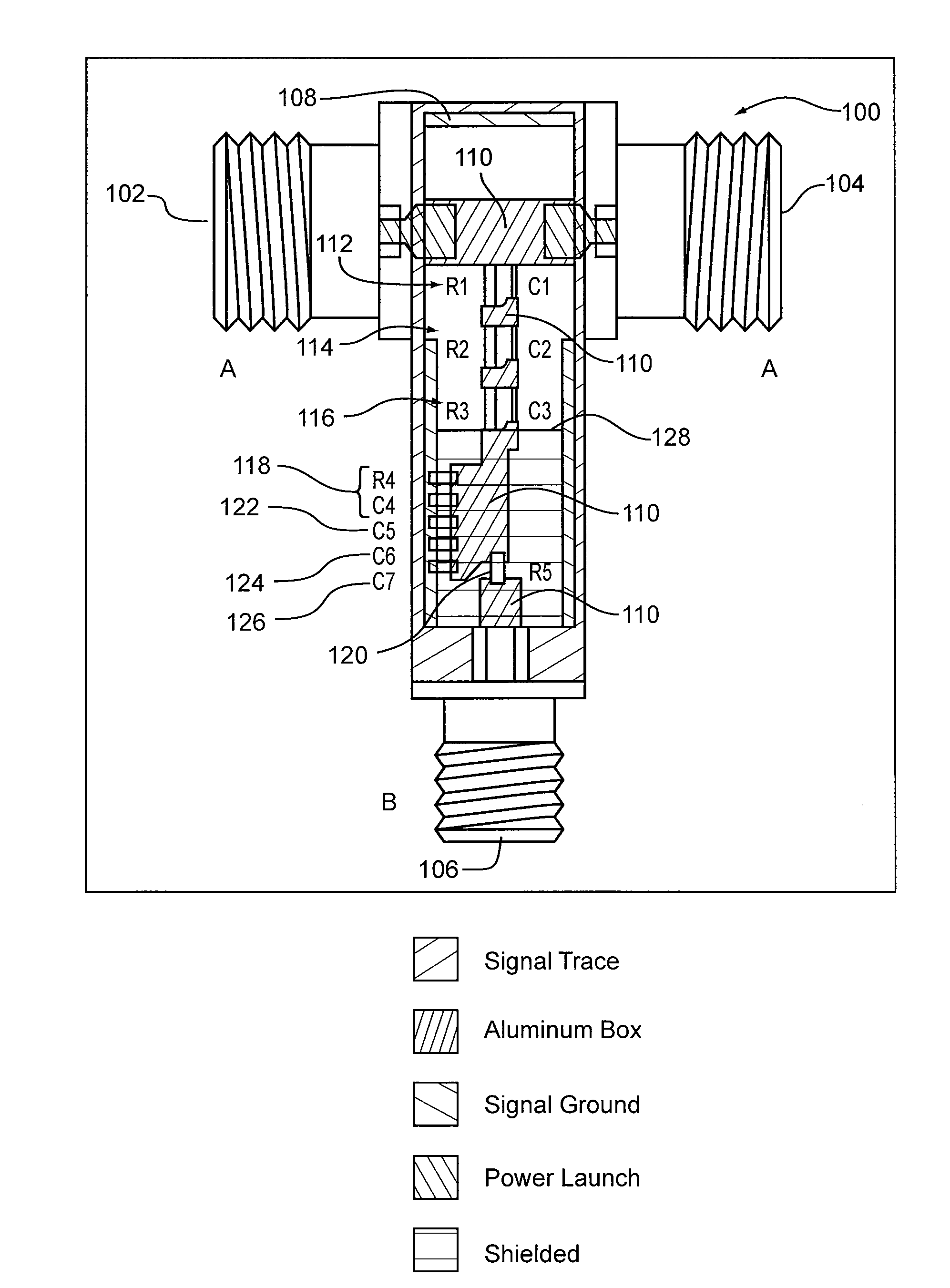
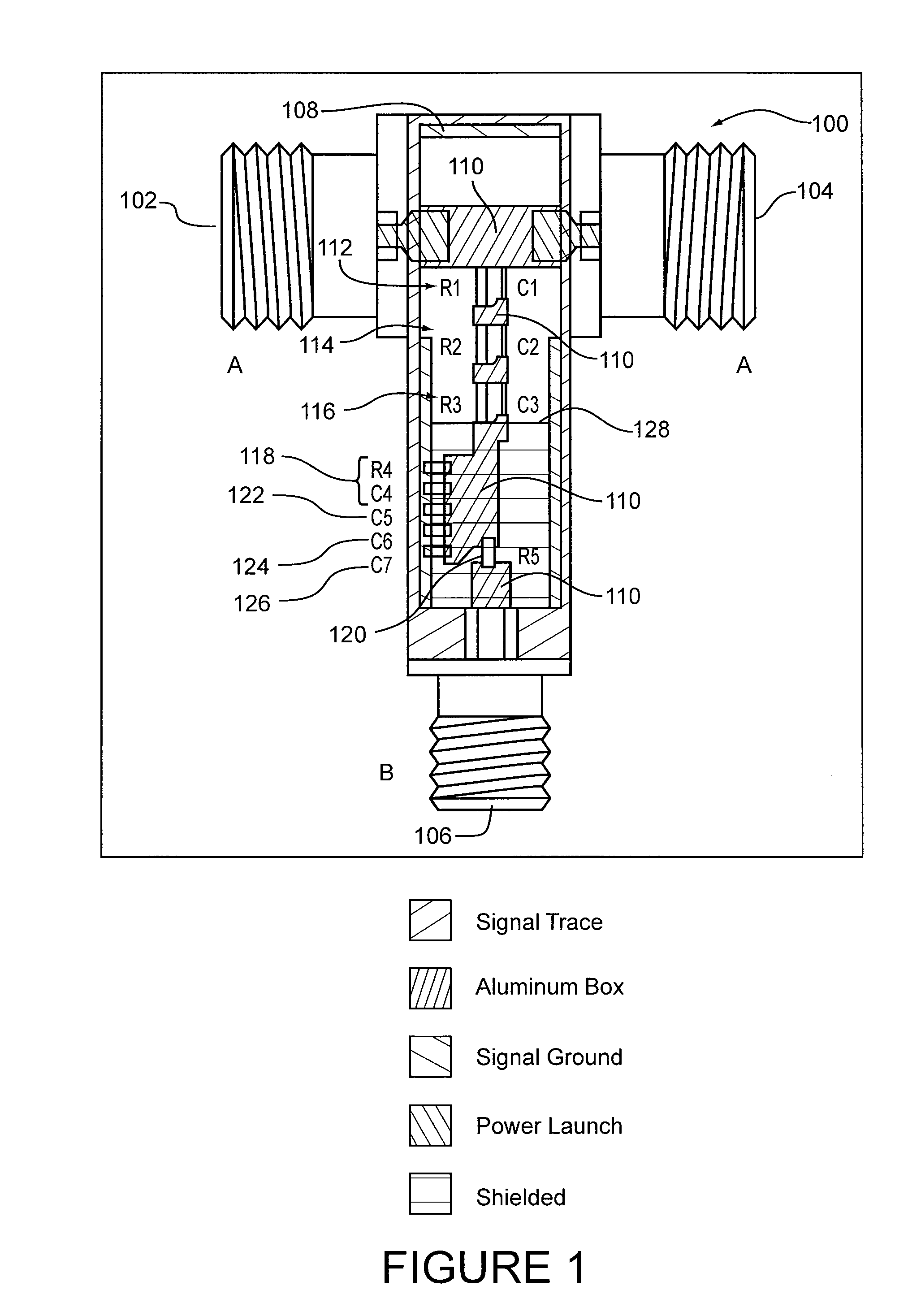
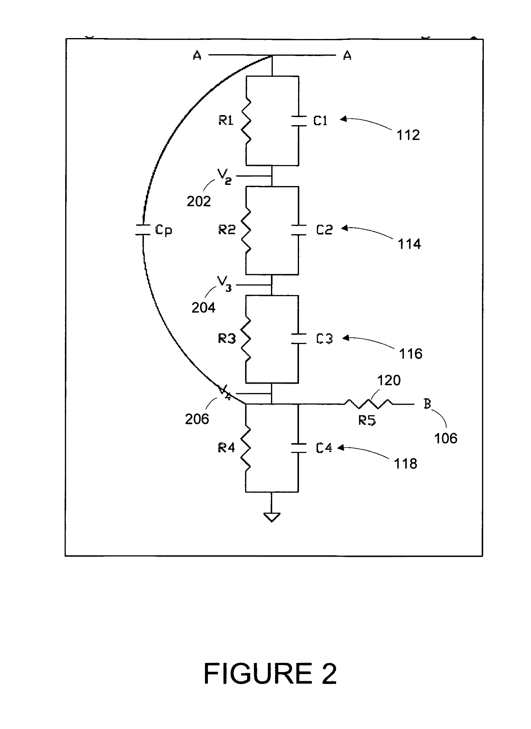
[0021]In-situ measuring or pickoff devices may interface open or closed networks (or circuits). The systems measure output with little magnitude or phase distortion with respect to frequency. Some devices have large dynamic ranges (e.g., single volts, kilo-volts, mega-volts, etc.) that interface one or more circuits. Some measuring devices do not require separate power sources and are not susceptible to electro-static discharge damage or over-voltage conditions. Due to shielded enclosures, high density layouts, and / or high output ranges, there may be little need for large amounts of insulation or warnings against shock when operating these systems. The pickoff devices may provide low parasitic capacitance (e.g., Cp≅0) and high linear input impedances. The devices may achieve improved high frequency responses and lower loading than alternative passive and / or active measuring devices.

[0022]The in-situ measuring or pickoff device may include two or more interfaces. In FIG. 1 the device...


PUM


Abstract

A measuring system minimizes the parasitic affects of lumped circuit elements. The system includes two or more in-situ interfaces configured to conductively link a source to an internal load and an external load. The in-situ interfaces are linked to a shunt conductor. Two or more linear and dynamic elements conductively link the in-situ interfaces in series. The dynamic elements are configured to overwhelm the parasitic self-capacitance of an input circuit coupled to at least one of the in-situ interfaces. A shield enclosing at least one of the linear and dynamic elements has a conductive surface to fields and electromagnetic interference. The shield has attenuation ratios that substantially dampen the parasitic capacitance between the linear and dynamic elements that bridge some of the in-situ interfaces.

Description

BACKGROUND OF THE INVENTION[0001]1. Technical Field[0002]This application relates to a closed circuit, and more particularly to a broad band multi-terminal network that mitigates parasitic elements.[0003]2. Related Art[0004]Electromagnetic signals within a wideband may be distorted by reactive elements. The inductance and capacitance within a circuit may distort the frequency and phase response of high frequency inputs or communication signals. Parasitic elements may affect inputs and outputs by reducing bandwidth or by creating unwanted oscillations and ringing.[0005]Unwanted inductance and capacitance may occur through links that connect electronic components or by their proximity to each other. Measurement systems that display voltage across or current passing through these components may add interference. Such circuits may require open access to measure inputs or outputs and distort waveforms or signals through their parasitic capacitance and low direct current resistance.SUMMAR...

Claims


Application Information

Patent Timeline
Patent Type & Authority Patents(United States)
IPC IPC(8): G01R27/28H04B3/28
CPCG01R15/06G01R1/0416
Inventor DEIBELE, CRAIG E.LINK, GEORGE BRIANPEPLOV, VLADIMIR V.
Owner UT BATTELLE LLC
Learn More