Semiconductor device and manufacturing method thereof

a semiconductor and semiconductor technology, applied in the direction of transistors, solid-state devices, transportation and packaging, etc., can solve the problems of reducing yield, deteriorating operating characteristics of thin-film transistors, and reducing reliability, so as to reduce adverse effects on semiconductor devices due to characteristics of the end portion of the semiconductor layer, reduce defects, and improve reliability

Inactive Publication Date: 2011-11-29
SEMICON ENERGY LAB CO LTD
View PDF47 Cites 10 Cited by
  • Summary
  • Abstract
  • Description
  • Claims
  • Application Information

AI Technical Summary

Benefits of technology

[0010]Because of such a problem due to the end portion of the island-shaped semiconductor layer, operating characteristics of a thin film transistor are deteriorated and the reliability is also reduced. Further, yield is also reduced in manufacturing semiconductor devices. The present invention is made in view of the foregoing problems, and an object of the present invention is to provide a semiconductor device having a novel structure with which the reliability is increased, as well as a manufacturing method thereof.
[0028]By employing the present invention, defects due to an end portion of a semiconductor layer can be reduced. Therefore, an adverse effect on a semiconductor device due to characteristics of the end portion of the semiconductor layer can be reduced, whereby a semiconductor device in which the reliability is improved can be provided. Further, in manufacturing a semiconductor device, the yield can be improved.

Problems solved by technology

Because of such a problem due to the end portion of the island-shaped semiconductor layer, operating characteristics of a thin film transistor are deteriorated and the reliability is also reduced.
Further, yield is also reduced in manufacturing semiconductor devices.

Method used


Image

  • Semiconductor device and manufacturing method thereof
  • Semiconductor device and manufacturing method thereof
  • Semiconductor device and manufacturing method thereof

Examples


embodiment mode 1

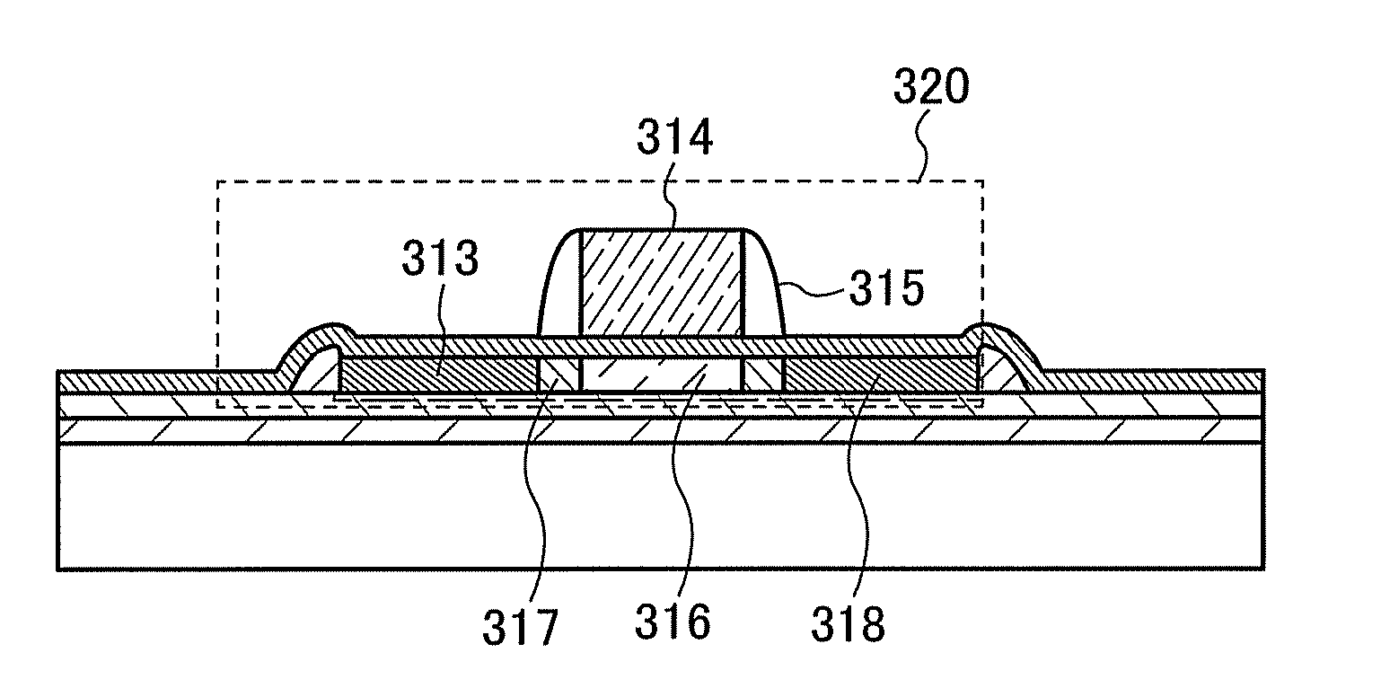
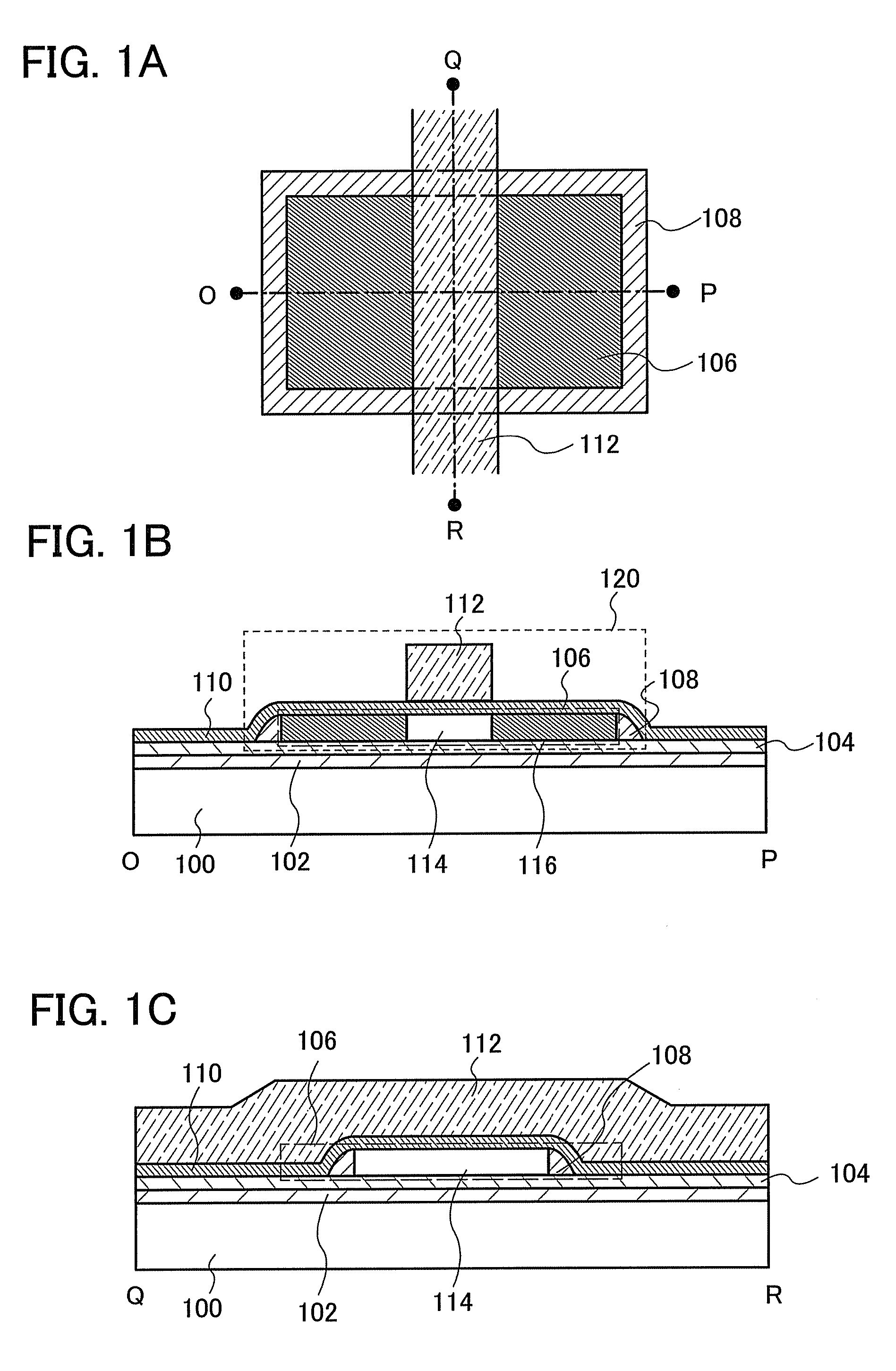
[0058]FIG. 1A is a top diagram and FIGS. 1B and 1C are cross-sectional diagrams for describing a main structure of a semiconductor device of the present invention. FIGS. 1A to 1C particularly show a structure of a thin film transistor; FIG. 1A is a top diagram, FIG. 1B is a cross-sectional diagram along a dashed line O-P in FIG. 1A, and FIG. 1C is a cross-sectional diagram along a dashed line Q-R in FIG. 1A. Note that a thin film and the like are partially omitted in FIG. 1A.

[0059]A thin film transistor 120 shown in FIG. 1A is provided over a substrate 100 having an insulating surface. The thin film transistor 120 includes a semiconductor layer 106, an insulating layer 108 which is provided so as to be in contact with a side surface of the semiconductor layer 106, an insulating layer 110 which is provided over one surface of the semiconductor layer 106, and a conductive layer 112 which is provided over the semiconductor layer 106 with the insulating layer 110 interposed therebetween...

embodiment mode 2

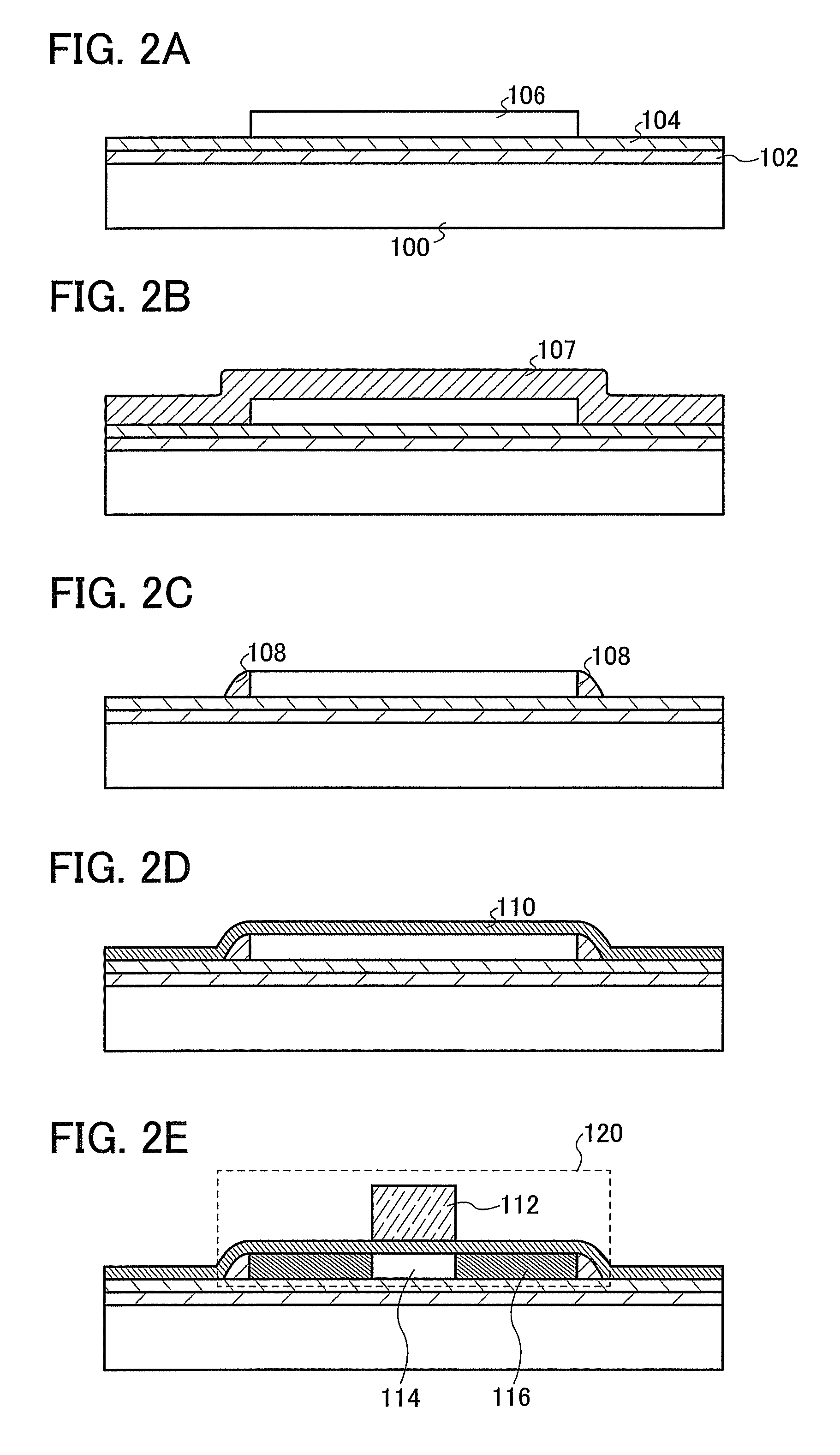
[0110]In this embodiment mode, an example of manufacturing a semiconductor device by a manufacturing method which is different from that in Embodiment Mode 1 is described with reference to FIGS. 3A to 3E.

[0111]First, a first semiconductor layer 306 is formed over a substrate 300, with an insulating layer 302 and an insulating layer 304 that function as a base insulating layer interposed therebetween (see FIG. 3A). Next, a first insulating layer 308 is formed to cover the first semiconductor layer 306 (see FIG. 3B). Note that up to and including the formation of the first insulating layer 308, the description made on the substrate 100, the insulating layer 102, the insulating layer 104, the semiconductor layer 106, and the first insulating layer 107 in Embodiment Mode 1 can be referred to, and therefore, a rough description thereof is made below.

[0112]As the substrate 300, a substrate having an insulating surface such as a glass substrate or a quartz substrate can be used. Each of th...

embodiment mode 3

[0146]In this embodiment mode, an example of manufacturing a semiconductor device by a manufacturing method that is different from that of foregoing Embodiment Mode 1 is described with reference to FIGS. 5A to 5E.

[0147]First, a first semiconductor layer 406 is formed over a substrate 400 with an insulating layer 402 and an insulating layer 404 that function as a base insulating layer interposed therebetween (see FIG. 5A). Next, a first insulating layer 408 is formed to cover the first semiconductor layer 406 (see FIG. 5B). Up to and including the formation of the first insulating layer 408, the description made on the substrate 100, the insulating layer 102, the insulating layer 104, the semiconductor layer 106, and the insulating layer 107 in Embodiment Mode 1 can be referred to, and therefore, the description thereof is roughly made below.

[0148]As the substrate 400, a substrate having an insulating surface such as a glass substrate or a quartz substrate can be used. Each of the in...


PUM


Abstract

An object is to provide a semiconductor device with improved reliability and for which a defect due to an end portion of a semiconductor layer provided in an island-shape is prevented, and a manufacturing method thereof. A structure includes an island-shaped semiconductor layer provided over a substrate, an insulating layer provided over a top surface and a side surface of the island-shaped semiconductor layer, and a gate electrode provided over the island-shaped semiconductor layer with the insulating layer interposed therebetween. In the insulating layer provided to be in contact with the island-shaped semiconductor layer, a region that is in contact with the side surface of the island-shaped semiconductor layer is made to have a lower dielectric constant than a region over the top surface of the island-shaped semiconductor layer.

Description

BACKGROUND OF THE INVENTION[0001]1. Field of the Invention[0002]The present invention relates to a semiconductor device and a manufacturing method thereof.[0003]2. Description of the Related Art[0004]In recent years, manufacturing of semiconductor devices, in which thin film transistors are formed over substrates of glass or the like having insulating surfaces and these thin film transistors are utilized as switching elements or the like, has been actively pursued. For these thin film transistors, island-shaped semiconductor layers are formed over a substrate having an insulating surface, and a part of the island-shaped semiconductor layers are utilized as channel forming regions (for example, see Patent Document 1: Japanese Published Patent Application No. H11-258636).[0005]Pattern diagrams of a general thin film transistor are FIGS. 12A to 12C. FIG. 12A is a top diagram of the thin film transistor, FIG. 12B is a cross-sectional diagram along a dashed line O-P, and FIG. 12C is a cr...

Claims


Application Information

Patent Timeline
Patent Type & Authority Patents(United States)
IPC IPC(8): H01L29/04
CPCH01L27/12H01L29/78675H01L29/66757Y10T428/24421
Inventor IKEDA, KAZUKOSASAGAWA, SHINYASUZAWA, HIDEOMIYAMAZAKI, SHUNPEI
Owner SEMICON ENERGY LAB CO LTD
Why Eureka
Try Eureka