System and method for model based multi-patterning optimization

a multi-pattern optimization and optimization system technology, applied in the field of integrated circuit design and manufacture, can solve the problems of limiting the effectiveness of current photolithographic processes, limited light/optics band, and other physical manufacturing constraints,

Active Publication Date: 2011-11-29
CADENCE DESIGN SYST INC
View PDF28 Cites 31 Cited by
  • Summary
  • Abstract
  • Description
  • Claims
  • Application Information

AI Technical Summary

Problems solved by technology

However, constraining factors in traditional photolithographic processes limit the effectiveness of current photolithographic processes.
Specifically, the lights / optics are band limited due to physical limitations (e.g., wavelength and aperture) of the photolithographic process.
Therefore, the photolithographic process cannot print beyond a certain pitch, distance, and other such physical manufacturing constraints.
Depending on the photolithographic process at issue, factors such as optics and wavelengths of light or radiation restrict how small the pitch may be made before features can no longer be reliably printed to a wafer or mask.
As such, the smallest size of any features that can be created on a wafer is severely limited by the pitch.
As a result, increasing feature densities beyond a certain threshold is infeasible via a pitch constrained single exposure process.
However, these and other techniques are limited both by cost and effectiveness.
However, design layouts with more sophisticated geometries (e.g., logic designs and microprocessor designs containing complex patterns and shapes with bends and jogs) cannot be processed using these existing decomposition tools as solutions do not exist for the unique patterns appearing within such design layouts.
Moreover, existing decomposition tools are inefficient in the manner by which they perform decomposition analysis.
Therefore, the more dense a design layout, the more time and processing resources needed to process and decompose the design layout.
Also, traditional prior art decomposition tools often operate in a local area by local area basis such that solutions provided to remedy printability issues appearing within a particular local area may have a detrimental effect to other unprocessed or processed local areas of the layout.

Method used


Image

  • System and method for model based multi-patterning optimization
  • System and method for model based multi-patterning optimization
  • System and method for model based multi-patterning optimization

Examples


Embodiment Construction

[0045]In the following description, numerous details are set forth for purpose of explanation. However, one of ordinary skill in the art will realize that the invention may be practiced without the use of these specific details. In other instances, well-known structures and devices are shown in block diagram form in order not to obscure the description of the invention with unnecessary detail.

I. Overview

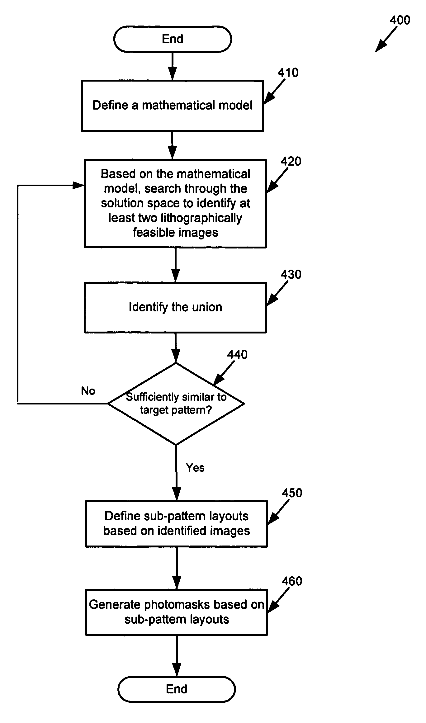
[0046]Some embodiments provide a process for decomposing a particular pattern on a layer of a design layout into multiple patterns that can be produced in multiple photolithographic operations for fabricating an integrated circuit (IC). FIG. 4 illustrates one example of such a process for some embodiments of the invention. As shown in FIG. 4, the process 400 initially defines (at 410) a model that expresses the range of feasible solutions for decomposing the particular pattern. In some embodiments, the model expresses the range of feasible solutions mathematically. In some embodiment...


PUM


Abstract

Some embodiments provide a method for optimally decomposing patterns within particular spatial regions of interest on a particular layer of a design layout for a multi-exposure photolithographic process. Specifically, some embodiments model the spatial region using a mathematical equation in terms of two or more intensities. Some embodiments then optimize the model across a set of feasible intensities. The optimization yields a set of intensities such that the union of the patterns created / printed from each exposure intensity most closely approximates the patterns within the particular regions. Based on the set of intensities, some embodiments then determine a decomposition solution for the patterns that satisfies design constraints of a multi-exposure photolithographic printing process. In this manner, some embodiments achieve an optimal photolithographic printing of the particular regions of interest without performing geometric rule based decomposition.

Description

FIELD OF THE INVENTION[0001]The invention relates to the design and manufacture of integrated circuits. Specifically, the invention relates to systems and methods for improving the photolithographic printability of an integrated circuit design layout.BACKGROUND OF THE INVENTION[0002]An integrated circuit (“IC”) is a device (e.g., a semiconductor device) or electronic system that includes many electronic components, such as transistors, resistors, diodes, etc. These components are often interconnected to form multiple circuit components, such as gates, cells, memory units, arithmetic units, controllers, decoders, etc. An IC includes multiple layers of wiring that interconnect its electronic and circuit components.[0003]Design engineers design ICs by transforming logical or circuit descriptions of the ICs' components into geometric descriptions, called design layouts. IC design layouts typically include (1) circuit modules (i.e., geometric representations of electronic or circuit IC c...

Claims


Application Information

Patent Timeline
Patent Type & Authority Patents(United States)
IPC IPC(8): G06F17/50
CPCG03F1/144G03F7/70466G03F1/70
Inventor GHAN, JUSTINSEZGINER, ABDURRAHMAN
Owner CADENCE DESIGN SYST INC
Why Eureka
Try Eureka