Image display device and method of driving the same

a technology of image display and display device, which is applied in the direction of static indicating device, instruments, etc., can solve the problems of insufficient correction of image quality degradation, and achieve the effects of preventing emission luminance dispersion, reducing gate-to-source voltage, and reducing threshold voltag

Active Publication Date: 2011-12-13
JOLED INC
View PDF20 Cites 0 Cited by
  • Summary
  • Abstract
  • Description
  • Claims
  • Application Information

AI Technical Summary

Benefits of technology

[0044]Therefore, when at a time period from the time point t2 to the time point t3 which can be allocated to the pixels for one line becomes short, for example, owing to the high resolution promotion, in the pixel circuit 5, it becomes difficult to properly set the voltage developed across the opposite terminals of the hold capacitor Cs at the threshold voltage Vth of the drive transistor Tr3. As a result, in the pixel circuit 5, it becomes impossible to sufficiently correct the deterioration of the image quality due to the dispersion of the threshold voltages Vth of the drive transistors Tr3. Therefore, in such a case, by applying the technique disclosed in Patent Document 2, the processing for setting the voltage developed across the opposite terminals of the hold capacitor Cs at the threshold voltage Vth of the drive transistor Tr3 is executed for multiple time periods, thereby making it possible to prevent the deterioration of the image quality.
[0059]According to either the embodiment or the another embodiment of the present invention, by holding the gate-to-source voltage of the drive transistor by the hold capacitor, the light emitting element can be driven so as to emit a light with the drive current corresponding to the voltage developed across the terminals of the hold capacitor by the driving operation of the drive transistor. In addition, after the voltage developed across the terminals of the hold capacitor is set at the voltage equal to or higher than the threshold voltage of the drive transistor, the electric charges corresponding to the voltage developed across the terminals of the hold capacitor are discharged, thereby setting the voltage developed across the terminals of the hold capacitor at the threshold voltage of the drive transistor. After that, the voltage for gradation setting is set, thereby making it possible to prevent the emission luminances from dispersing due to the dispersion of the threshold voltages of the drive transistors. In addition, when the electric charges corresponding to the voltage developed across the terminals of the hold capacitor are discharged through the drive transistor, for the time period for which the voltage of the corresponding one of the signal lines is set at the voltage for gradation setting, the write transistor is turned OFF, which results in that the processing for discharging the electric charges corresponding to the voltage developed across the terminals of the hold capacitor through the drive transistor is executed for the multiple time periods for each of which the voltage of the corresponding one of the signal lines is set at the fixed voltage. As a result, the electric charges corresponding to the voltage developed across the terminals of the hold capacitor can be discharged for the sufficient time period ensured. Thus, it is possible to cope with the high resolution promotion or the like. In addition, when the write transistor is turned OFF for the time period for which the voltage of the corresponding one of the signal lines is set at the voltage for gradation setting, the voltage developed across the terminals of the hold capacitor is made variable from the fixed voltage by utilizing the running between the wiring patterns formed on the insulating substrate, thereby reducing the gate-to-source voltage of the write transistor. As a result, it is possible to prevent each of the gate voltage and the source voltage of the write transistor from rising for this time period without providing a special configuration. Therefore, the threshold voltage can be prevented from being failed, thereby reliably correcting the dispersion of the threshold voltages of the drive transistors.
[0060]According to embodiments of the present invention, the dispersion of the threshold voltages of the drive transistors can be reliably corrected even when the discharge of the electric charges corresponding to the voltage developed across the terminals of the hold capacitor through the drive transistor is carried out for the multiple time periods so as to correct the dispersion of the threshold voltages of the drive transistors by discharging the electric charges corresponding to the voltage developed across the terminals of the hold capacitor through the drive transistor.

Problems solved by technology

As a result, in the pixel circuit 5, it becomes impossible to sufficiently correct the deterioration of the image quality due to the dispersion of the threshold voltages Vth of the drive transistors Tr3.

Method used


Image

  • Image display device and method of driving the same
  • Image display device and method of driving the same
  • Image display device and method of driving the same

Examples


embodiment 1

(1) Constitution of Embodiment 1

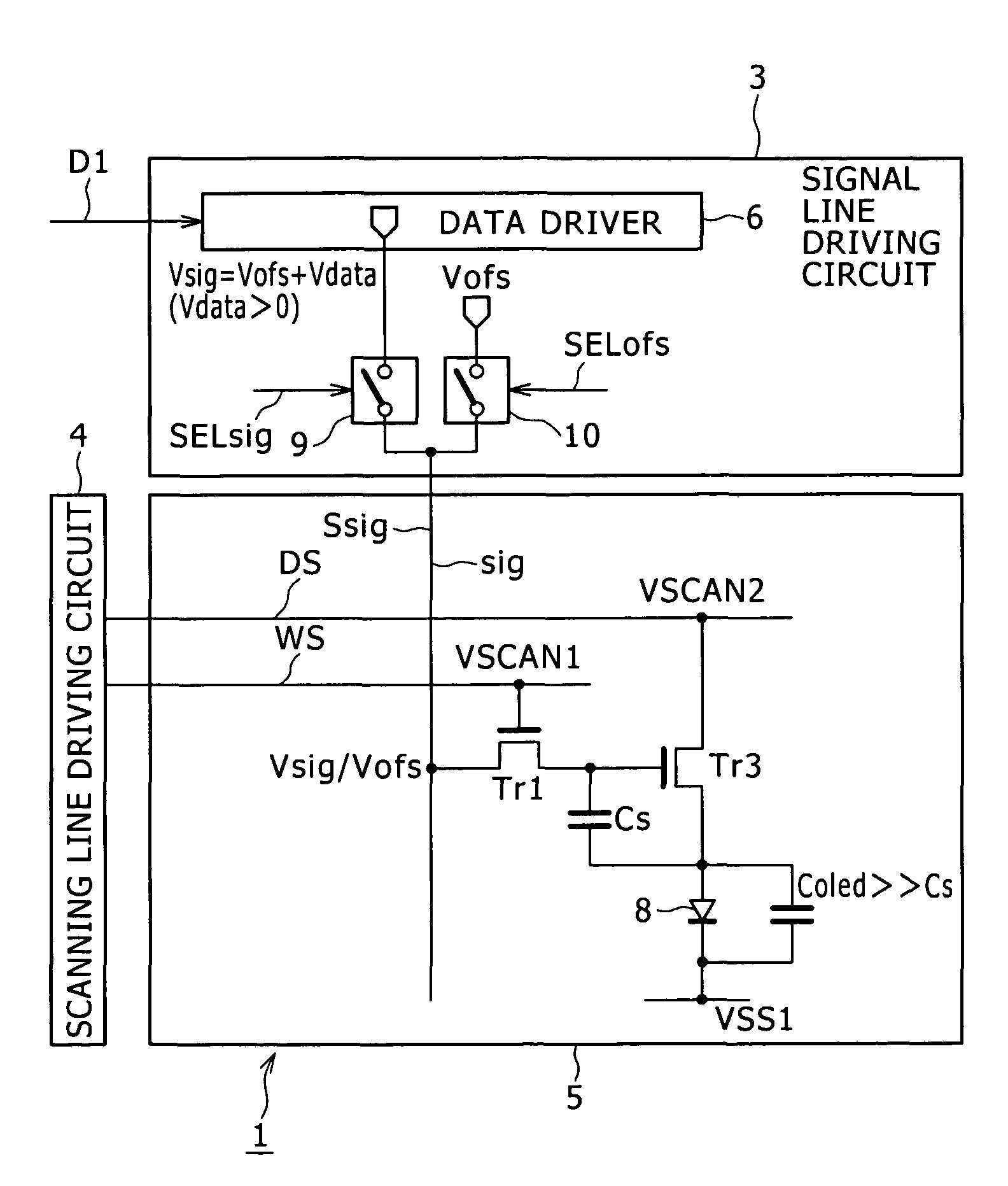
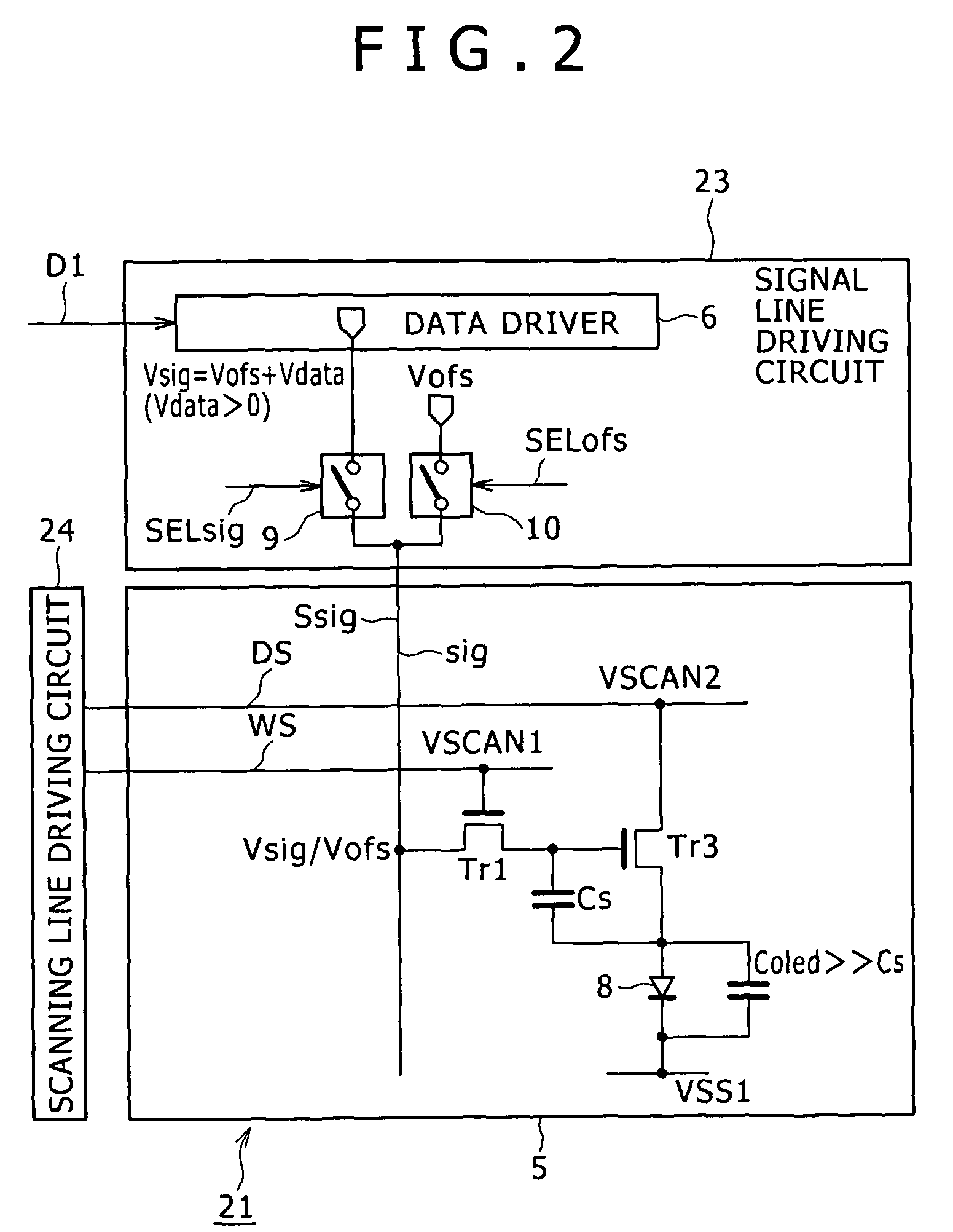
[0079]FIG. 2 is a circuit diagram, partly in block, showing a configuration of a pixel circuit which is applied to an image display device 21 according to Embodiment 1 of the present invention in contrast with the configuration of the pixel circuit in the existing image display device 1 shown in FIG. 13. The image display device 21 has the same configuration as that of the existing display device 1 described above except that a signal line driving circuit 23 and a scanning line driving circuit 24 are provided instead of providing the signal line driving circuit 3 and the scanning line driving circuit 4. Therefore, in the following description, portions corresponding to those shown in FIG. 13 are designated with the same reference numerals.

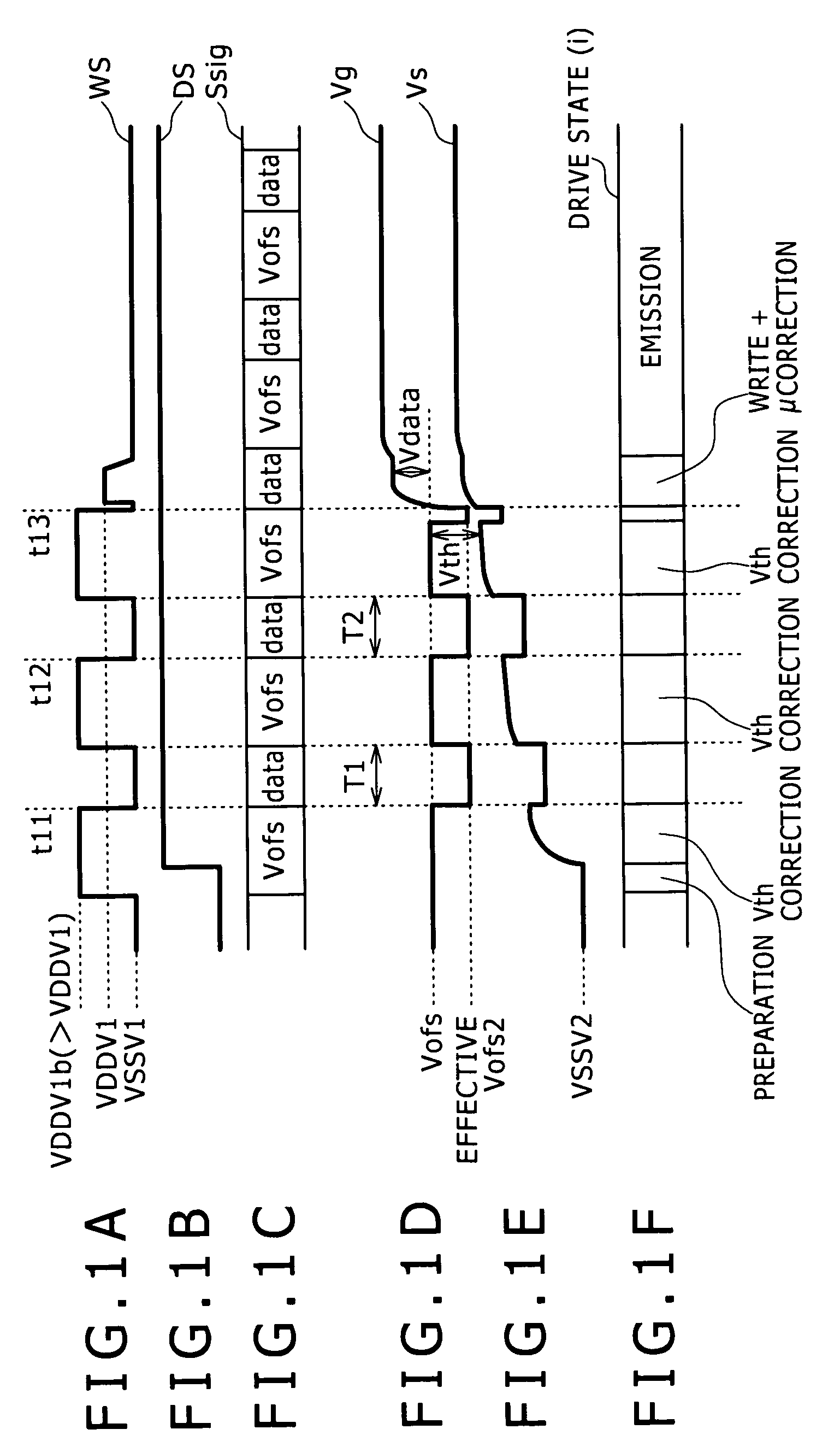
[0080]Here, the signal line driving circuit 23, as shown in FIG. 1C, outputs alternately a voltage Vsig (Vdata+Vofs) for gradation setting, and a fixed voltage Vofs for threshold voltage to a signal line sig similarl...

embodiment 2

[0110]FIGS. 3A to 3F are a time chart explaining an operation of a pixel circuit in an image display device according to Embodiment 2 of the present invention in contrast with the case of the operation of the pixel circuit explained with reference to FIGS. 1A to 1F. The image display device of Embodiment 2 has the same configuration as that of the image display device 21 of Embodiment 1 except that a configuration of a scanner 6A (refer to FIG. 12) concerned with generation of a write signal WS in a scanning line driving circuit is different from that of the scanner 6A in Embodiment 1. In addition, the image display device of Embodiment 2 has the same configuration as that of the image display device 21 of Embodiment 1 except that with regard to the scanner 6A, after being caused to rise with the large amplitude only with leading one cycle, the write signal WS is caused to drop with the large amplitude.

[0111]That is to say, when the voltage developed across the opposite terminals of...

embodiment 3

[0115]FIGS. 4A to 4F are a time chart explaining an operation of a pixel circuit in an image display device according to Embodiment 3 of the present invention in contrast with the case of the operation of the pixel circuit explained with reference to FIGS. 1A to 1F. The image display device of Embodiment 3 has the same configuration as that of the image display device 21 of Embodiment 1 except that a configuration of a scanner 6A (refer to FIG. 12) concerned with generation of a write signal WS in a scanning line driving circuit is different from that of the scanner 6A in Embodiment 1.

[0116]In addition, in Embodiment 3, with regard to the scanner 6A, for a time period for which the write signal is caused to drop with the large amplitude by switching from one of the voltages VSSV1 and VSSV1b to the other in the phase of the rising of the write signal WS, thereby setting the voltage of the signal line at the voltage for gradation setting, the gate voltage of the drive transistor is ca...


PUM


Abstract

An image display device includes a display portion formed by disposing pixel circuits in a matrix, and a signal line driving circuit and a scanning line driving circuit for driving the pixel circuits through signal lines and scanning lines of the display portion. The pixel circuit includes at least: a light emitting element; a drive transistor for current-driving the light emitting element by a drive current corresponding to a gate-to-source voltage thereof; a hold capacitor composed of either one capacitor or a plurality of coupling capacitors for holding therein the gate-to-source voltage; and a write transistor adapted to be turned ON / OFF in accordance with a write signal outputted from the scanning line driving circuit, thereby setting a voltage developed across terminals of the hold capacitor at a voltage of corresponding one of the signal line.

Description

BACKGROUND OF THE INVENTION[0001]1. Field of the Invention[0002]The present invention relates to an image display device and a method of driving the same. For example, the present invention can be applied to an active matrix type image display device using organic Electro Luminescence (EL) elements. In the present invention, the electric charges originating from which a voltage developed across opposite terminals of a hold capacitor are discharged through a drive transistor, thereby correcting a dispersion of threshold voltages of the drive transistors. In this case, a gate-to-source voltage of the drive transistor is reduced for a time period for which the discharge of the electric charges corresponding to the voltage developed across the opposite terminals of the hold capacitor is temporarily stopped by utilizing running between wiring patterns formed on a substrate. Thus, in the present invention, it is made possible to reliably correct the dispersion of the threshold voltages of...

Claims


Application Information

Patent Timeline
Patent Type & Authority Patents(United States)
IPC IPC(8): G09G3/30
CPCG09G3/3241G09G3/3275G09G2300/0819G09G2300/0866G09G2310/0256G09G2310/0262G09G2320/043G09G2300/0842G09G3/20G09G3/30G09G3/32G09G3/3233
Inventor ASANO, MITSURU
Owner JOLED INC
Why Eureka
Try Eureka