Check patentability & draft patents in minutes with Patsnap Eureka AI!

Substrate processing apparatus and substrate transfer method adopted in substrate processing apparatus

a substrate processing and substrate technology, applied in the field of substrate processing apparatus and substrate transfer method adopted in the substrate processing apparatus, can solve the problems of long wait time, inconvenient operation, and inability to meet the requirements of substrate processing, so as to reduce the length of wait time, and ensure the effect of processing speed

Active Publication Date: 2011-12-13
TOKYO ELECTRON LTD
View PDF12 Cites 6 Cited by
  • Summary
  • Abstract
  • Description
  • Claims
  • Application Information

AI Technical Summary

Benefits of technology

This approach improves the operation rates of individual processing chambers and overall throughput by ensuring wafers are transferred efficiently, reducing wait times and eliminating unnecessary idle periods, thereby enhancing the processing efficiency of the substrate processing apparatus.

Problems solved by technology

Thus, the lengths of time required to process a single wafer in the various processing chambers, the length of time to elapse after a wafer is delivered into a given processing chamber until the wafer processing is completed and the wafer is transferred out of the processing chamber so that the processing chamber becomes available for the next wafer, are not always uniform.
Under such circumstances, the transfer system in the related art may become counterproductive and reduce both the operation rates of the individual processing chambers and the throughput of the substrate processing apparatus.
As a result, an unnecessary idle time occurs in the processing chamber P2 with the shorter processing time, which reduces the operation rate of the processing chamber P2 to lead to a reduction in the throughput of the substrate processing apparatus.

Method used


Image

  • Substrate processing apparatus and substrate transfer method adopted in substrate processing apparatus
  • Substrate processing apparatus and substrate transfer method adopted in substrate processing apparatus
  • Substrate processing apparatus and substrate transfer method adopted in substrate processing apparatus

Examples


Embodiment Construction

[0042]The following is a detailed explanation of preferred embodiments of the present invention, given in reference to the attached drawings. It is to be noted that in the specification and the drawings, the same reference numerals are assigned to components having substantially identical functions and structural features to preclude the necessity for a repeated explanation thereof.

[0043](Structural Example Adopted in Substrate Processing Apparatus)

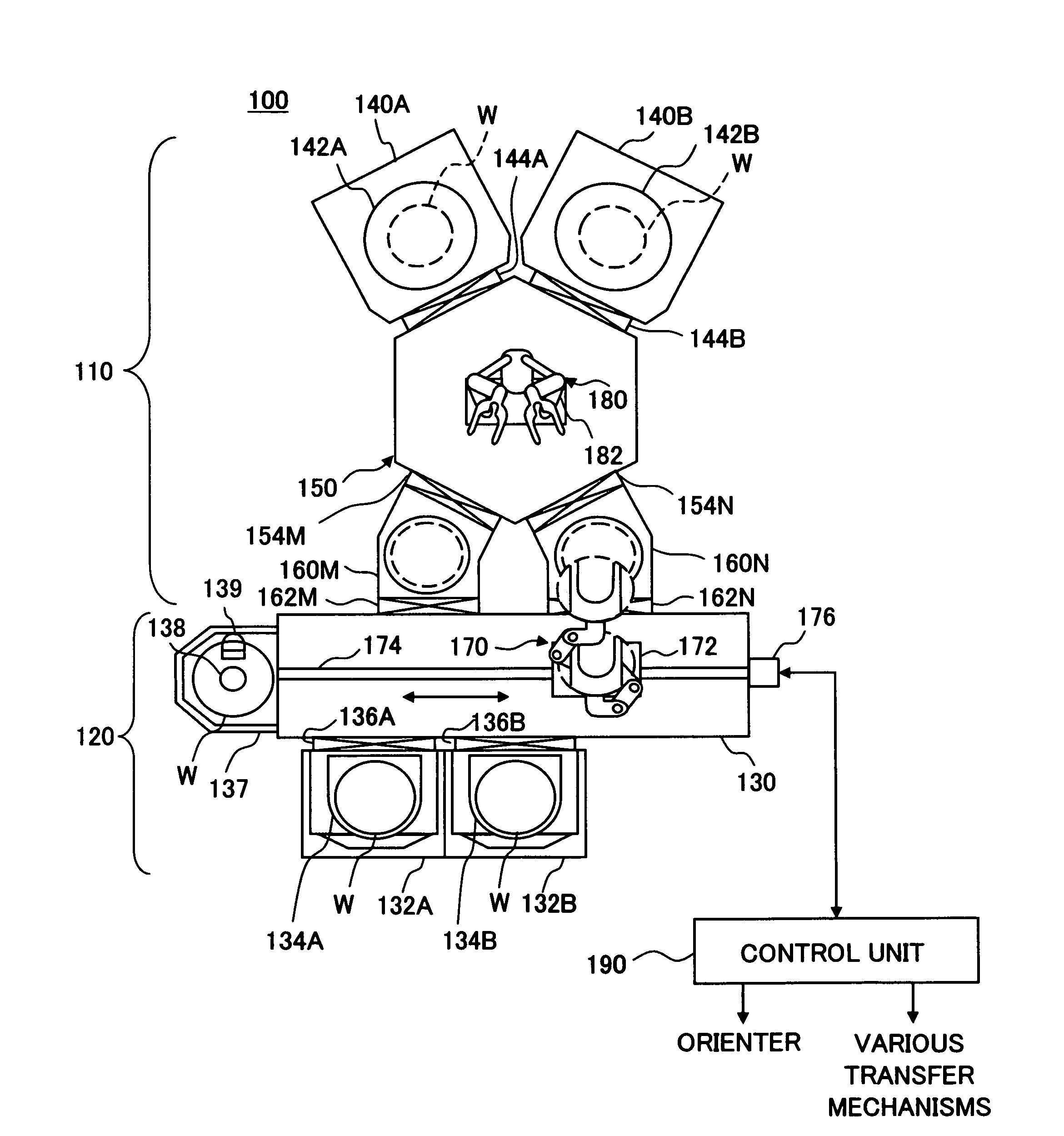
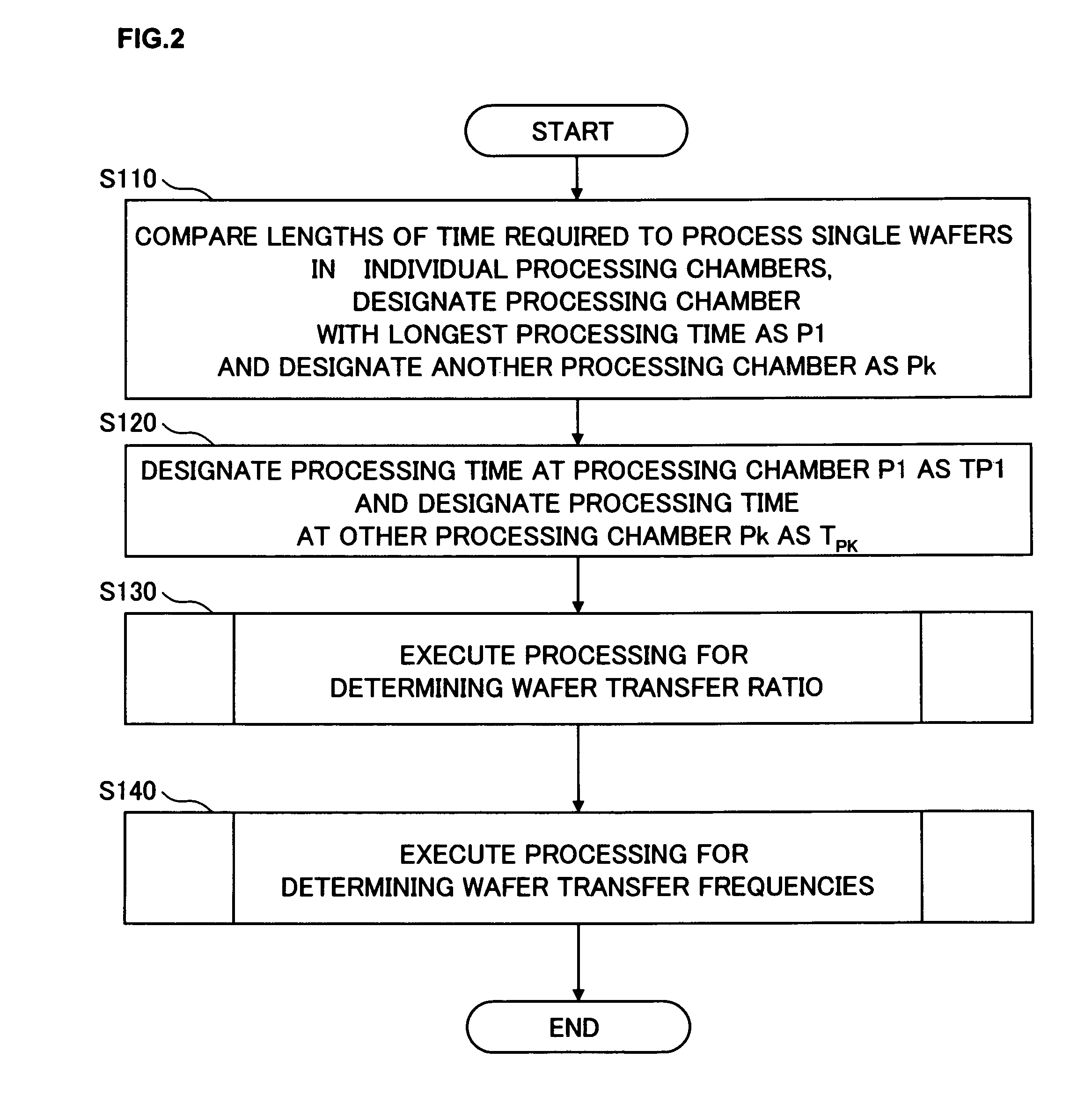
[0044]First, the substrate processing apparatus achieved in an embodiment of the present invention is explained in reference to drawings. FIG. 1 schematically shows the structure adopted in the substrate processing apparatus in an embodiment of the present invention. The substrate processing apparatus 100 comprises a processing unit 110 where various types of processing such as film formation and etching are executed on substrates which may be, for instance, semiconductor wafers (hereafter may be simply referred to as “wafers”) W and a tr...


PUM


Abstract

In a substrate processing apparatus according to the present invention, wafer transfer timing with which wafers are to be transferred to individual processing chambers from a cassette container is determined in correspondence to each processing chamber, based upon the lengths of time required to process a single wafer in the processing chambers. Then, wafers are transferred from the cassette container in conformance to the transfer timing thus determined. By setting the wafer transfer timing with which wafers are transferred from the cassette container in coordination with the lengths of processing time at the individual processing chambers, the operation rates in the processing chambers are improved and ultimately, the throughput of the apparatus is improved.

Description

CROSS REFERENCE TO RELATED APPLICATIONS[0001]This document claims priority to Japanese Patent Application No. 2004-352796, filed Dec. 6, 2004 and U.S. Provisional Application No. 60 / 663,262 filed Mar. 21, 2005, the entire contents of which are hereby incorporated by reference.FIELD OF THE INVENTION[0002]The present invention relates to a substrate processing apparatus used to execute a specific type of processing on a substrate to be processed (to be referred to simply as substrate subsequently) such as a semiconductor wafer or a glass substrate (e.g., a liquid crystal substrate) and a substrate transfer method that may be adopted in the substrate processing apparatus.BACKGROUND OF THE INVENTION[0003]A substrate processing apparatus used for the purposes described above normally comprises a processing unit that includes a plurality of processing chambers where a specific type of processing is executed on substrates such as semiconductor wafers (hereafter may be simply referred to as...

Claims


Application Information

Patent Timeline
Patent Type & Authority Patents(United States)
IPC IPC(8): G06F7/00
CPCH01L21/67196H01L21/67253Y10S414/135
Inventor OGI, TATSUYA
Owner TOKYO ELECTRON LTD
Features
  • R&D
  • Intellectual Property
  • Life Sciences
  • Materials
  • Tech Scout
  • Unparalleled Data Quality
  • Higher Quality Content
  • 60% Fewer Hallucinations
Learn More