Manufacturing method of semiconductor device

a manufacturing method and semiconductor technology, applied in the direction of solid-state devices, chemical vapor deposition coatings, coatings, etc., can solve the problems of affecting increasing contact resistance between plugs, and other problems, so as to improve the operation rate of multi-chamber film forming apparatus

Inactive Publication Date: 2008-07-24
RENESAS ELECTRONICS CORP
View PDF6 Cites 32 Cited by
  • Summary
  • Abstract
  • Description
  • Claims
  • Application Information

AI Technical Summary

Benefits of technology

[0019]The present invention makes it possible to avoid an inconvenience at a connection portion obtained by filling, in a connecting hole opened in an insulating film, a tungsten film via a barrier metal film composed of a titanium nitride film and a titanium film stacked one after another. The present invention also makes it possible to improve an operation rate of a multi-chamber type film forming apparatus to be used for the formation of the barrier metal film.

Problems solved by technology

The barrier metal film obtained by depositing a titanium nitride film on a titanium film and thus having a film stack structure has, however, various technological problems as will be described below.
This results in a rise in contact resistance between the plug and nickel silicide layer.
In addition to this problem, the barrier metal film has another problem.

Method used


Image

  • Manufacturing method of semiconductor device
  • Manufacturing method of semiconductor device
  • Manufacturing method of semiconductor device

Examples


Embodiment Construction

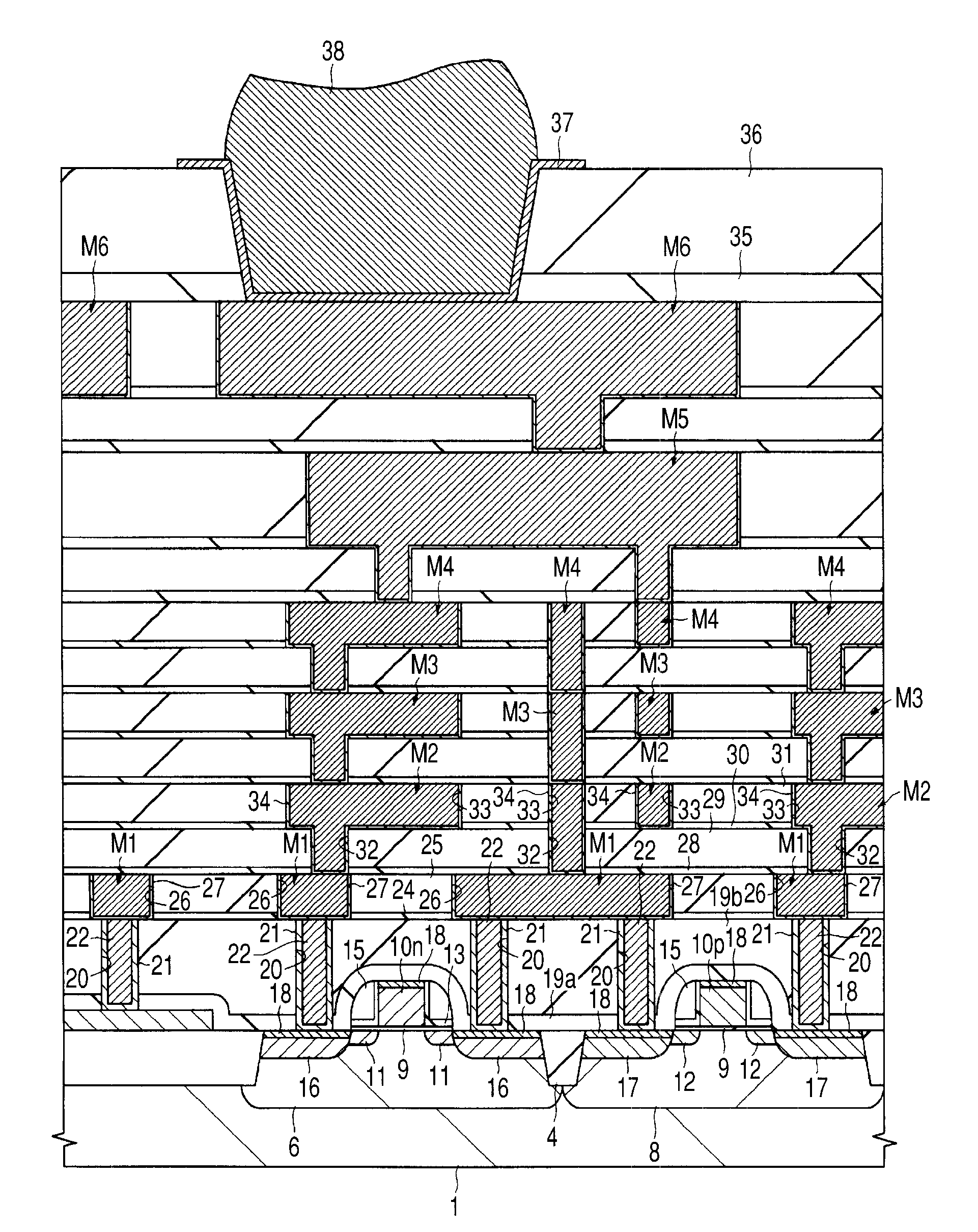
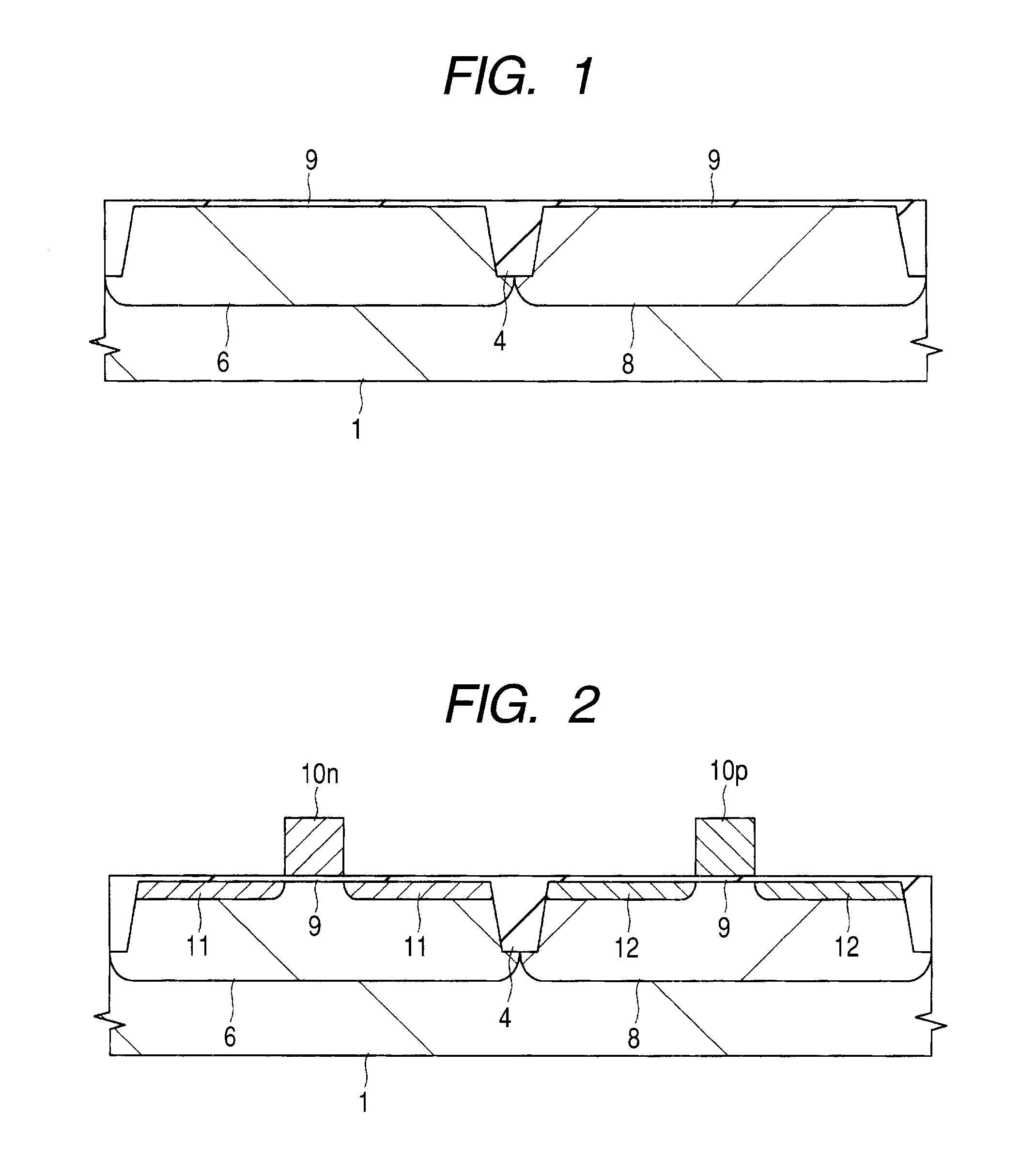
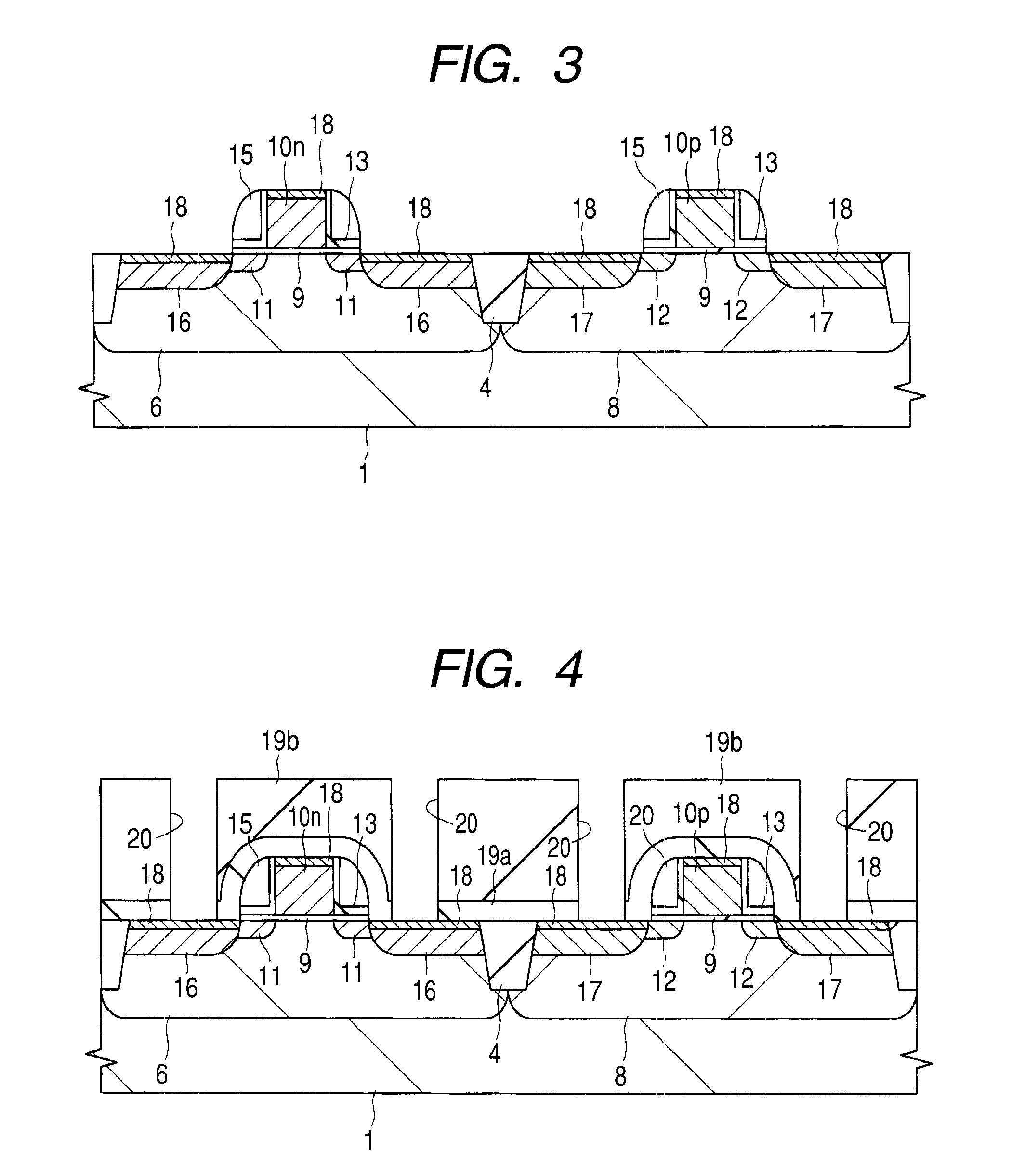
[0042]In the present embodiments, a description will be made after divided into plural sections or in plural embodiments if necessary for convenience sake. These plural sections or embodiments are not independent each other, but in relation such that one is a modification example, details or complementary description of a part or whole of the other one unless otherwise specifically indicated. And, in the present embodiments, when a reference is made to the number of elements (including the number, value, amount and range), the number is not limited to a specific number but may be greater than or less than the specific number, unless otherwise specifically indicated or principally apparent that the number is limited to the specific number. Further, in the present embodiments, it is needless to say that the constituting elements (including element steps) are not always essential unless otherwise specifically indicated or principally apparent that they are essential. Similarly, in the ...


PUM

PropertyMeasurementUnit
temperatureaaaaaaaaaa
thicknessaaaaaaaaaa
temperatureaaaaaaaaaa

Abstract

An object of the invention is to avoid an inconvenience at a connection portion formed by filling a metal film in a connecting hole, which has been opened in an insulating film, via a barrier metal film having a titanium nitride film stacked over a titanium film. A manufacturing method of a semiconductor device has the steps of: forming a thermal reaction Ti film over the bottom of a connecting hole by a thermal reaction using a TiCl4 gas; forming a plasma reaction Ti film by a plasma reaction using a TiCl4 gas; forming a nitrogen-rich TiN film over the surface of the plasma reaction Ti film by plasma treatment with H2 and plasma treatment with NH3 gases; repeatedly carrying out film formation by CVD using a WF6 gas and reduction using an SiH4 or B2H6 gas to form a tungsten nucleation film of a multilayer structure over the nitrogen-rich TiN film; and forming a blanket•tungsten film at 400° C. or less by CVD using WF6 and H2 gases. This makes it possible to avoid an inconvenience at a connection portion formed by filling a metal film in a connecting hole, which has been opened in an insulating film, via a barrier metal film having a titanium nitride film stacked over a titanium film.

Description

CROSS-REFERENCE TO RELATED APPLICATIONS[0001]The disclosure of Japanese Patent Application No. 2006-282100 filed on Oct. 17, 2006 including the specification, drawings and abstract is incorporated herein by reference in its entirety.BACKGROUND OF THE INVENTION[0002]The present invention relates to a manufacturing technology of a semiconductor device, in particular, to a technology effective when applied to one of the manufacturing steps of a semiconductor device, that is, filling a metal film, via a barrier metal film, in a connecting hole opened in an insulating film.[0003]In Japanese Patent Laid-Open No. 2004-363402, disclosed is a method of forming a Ti layer on at least the inner wall and bottom portion of a contact hole penetrating an insulating layer, nitriding the Ti layer with N radicals to form a TiN layer on the Ti layer, and filling a conductive layer in the contact hole (refer to Japanese Patent Laid-Open No. 2004-363402, Paragraphs [0026] to [0028], FIGS. 4 and 5).[0004...

Claims


Application Information

Patent Timeline
Patent Type & Authority Applications(United States)
IPC IPC(8): H01L21/768
CPCC23C16/14H01L2224/0401C23C16/45534C23C16/56H01L21/02063H01L21/28518H01L21/28556H01L21/76814H01L21/76843H01L21/76846H01L21/76856H01L21/76862H01L21/76876H01L24/02H01L24/12H01L2224/13144H01L2924/01078H01L2924/01079H01L2924/04941H01L2924/14H01L2224/0558H01L2224/05644C23C16/45523H01L21/28H01L21/3205
Inventor FUTASE, TAKUYAHAYASHI, TAKESHI
Owner RENESAS ELECTRONICS CORP
Why Eureka
Try Eureka