

High performance resonant element
a resonant element and high-performance technology, applied in the field of high-performance resonant elements, can solve the problems of restricting the frequency content of the signal that can be transmitted, stub vias are generally unavoidable, and stub vias are conventionally viewed as having very adverse effects upon signal propagation, so as to achieve low loss, low overall cost, and high-performance resonant
- Summary
- Abstract
- Description
- Claims
- Application Information
AI Technical Summary
Benefits of technology
Problems solved by technology
Method used
Image

Examples
Embodiment Construction
[0036]Referring now to the drawings, and more particularly to FIGS. 1-9, there are shown exemplary embodiments of the methods and systems of the present invention.
[0037]Stub vias may be classified into two types: an open stub via and a shorted stub via. An open stub via has an end, which is distally located with respect to associated signal lines and which is not connected to any other conductor. In contrast, a shorted stub via has an end, which is distally located with respect to the associated signal lines, and which is connected to a ground.
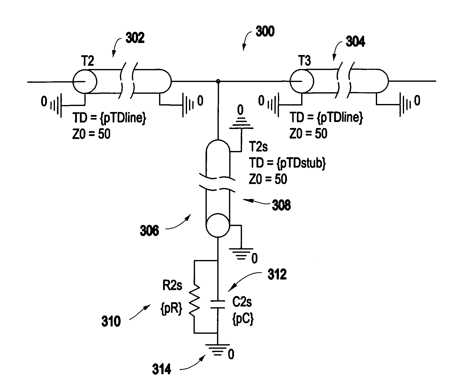
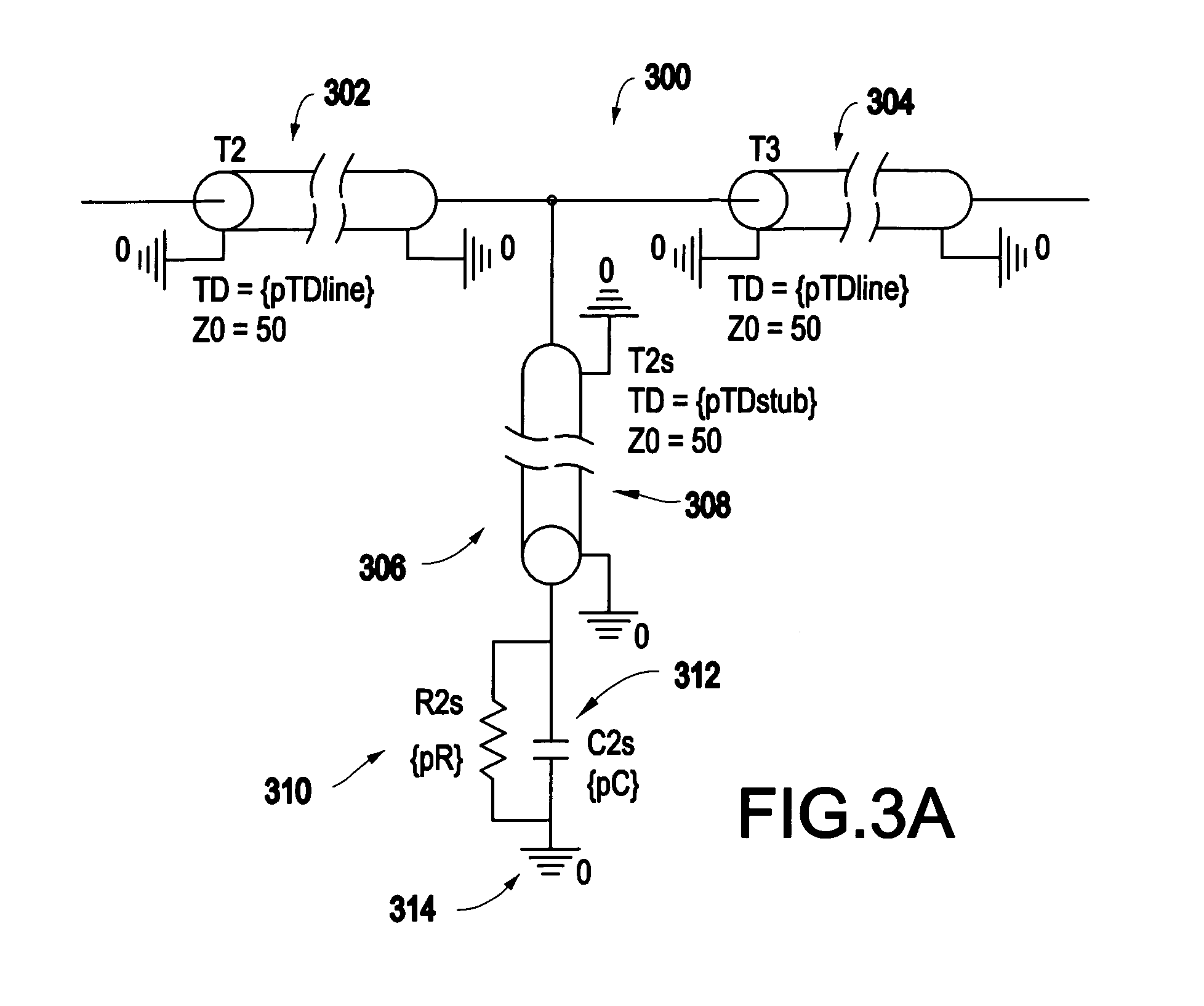
[0038]Propagation of a signal within a via segment, is often modeled as a propagation down a transmission line, which, in general possesses a different impedance from “real” signal lines. FIG. 3A illustrates a model 300 for a shorted-type via, and FIG. 3B illustrates a plot of a frequency response of the model of FIG. 3A.
[0039]The model 300 includes an input signal line 302, an output signal line 304, and a shorted-type via 306. The via portio...
PUM
 Abstract
Description
Claims
Application Information