Supercharge Your Innovation With Domain-Expert AI Agents!

Semiconductor device and method for fabricating the same

a semiconductor and semiconductor technology, applied in the field of semiconductor devices, can solve the problems of severe hot carrier effect, high gate-induced drain leakage current, etc., and achieve the effect of improving performan

Active Publication Date: 2012-01-10
MACRONIX INT CO LTD
View PDF10 Cites 4 Cited by
  • Summary
  • Abstract
  • Description
  • Claims
  • Application Information

AI Technical Summary

Benefits of technology

[0008]Accordingly, the present invention is directed to a semiconductor device with an enhanced performance.
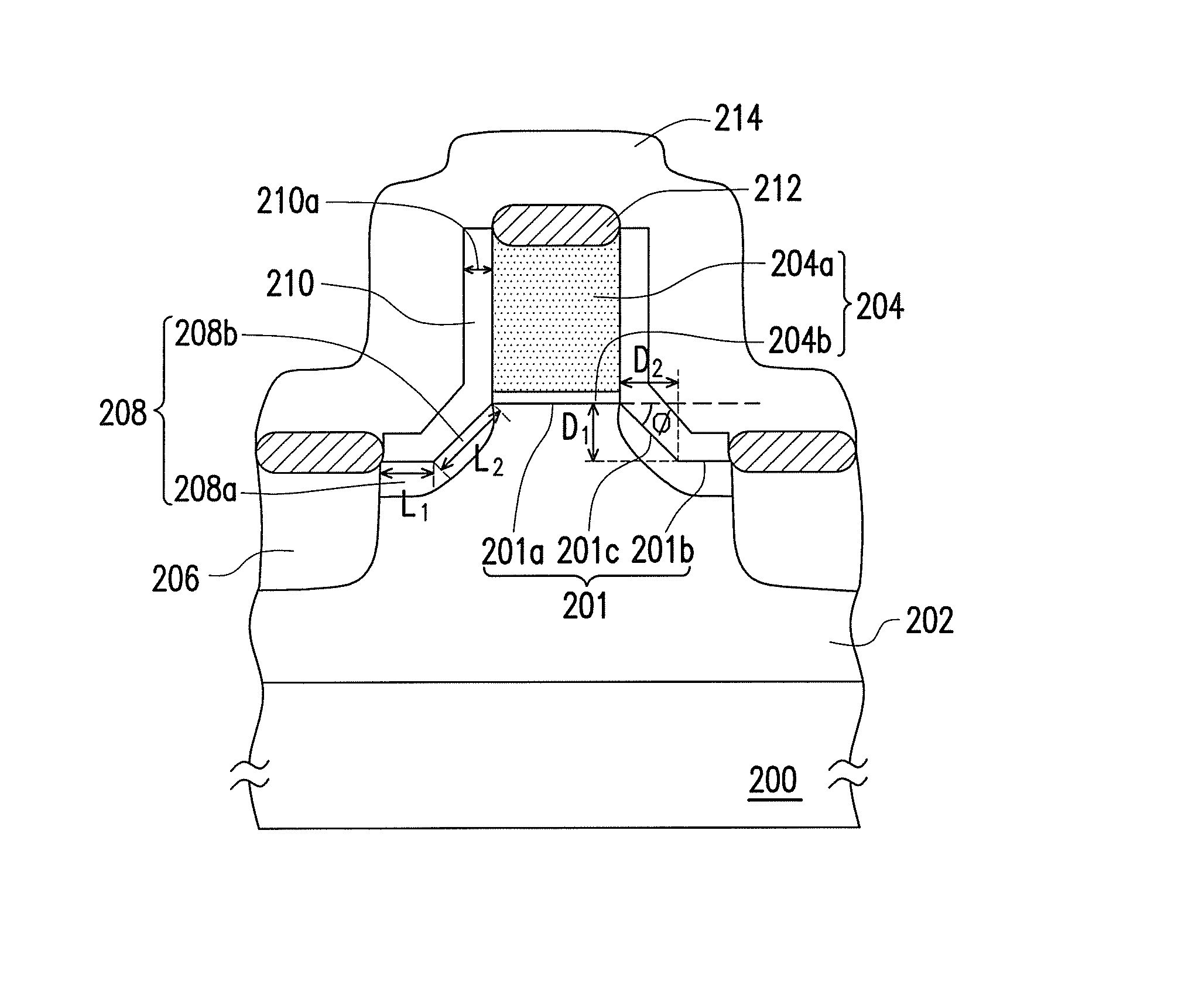
[0037]As mentioned above, the semiconductor device in the present invention has the lightly doped regions as SDE, and hot carrier effect can therefore be alleviated by the tilted and bended SDE without lightening the concentration of the lightly doped regions. Additionally, GIDL current and gate-drain overlap capacitance can be reduced due to the disposition of the tilted and bended SDE.
[0038]Moreover, the method for fabricating the semiconductor device in the present invention forms the lightly doped regions with a tilted and bended profile, so that the diffusion of the lightly doped regions is not affected by the doped regions thereby the spacer able to be thinner in this structure of the semiconductor device. Hence, the stress layer can be closer to the channel region and the performance of the device can be improved owing to the thinner spacer.

Problems solved by technology

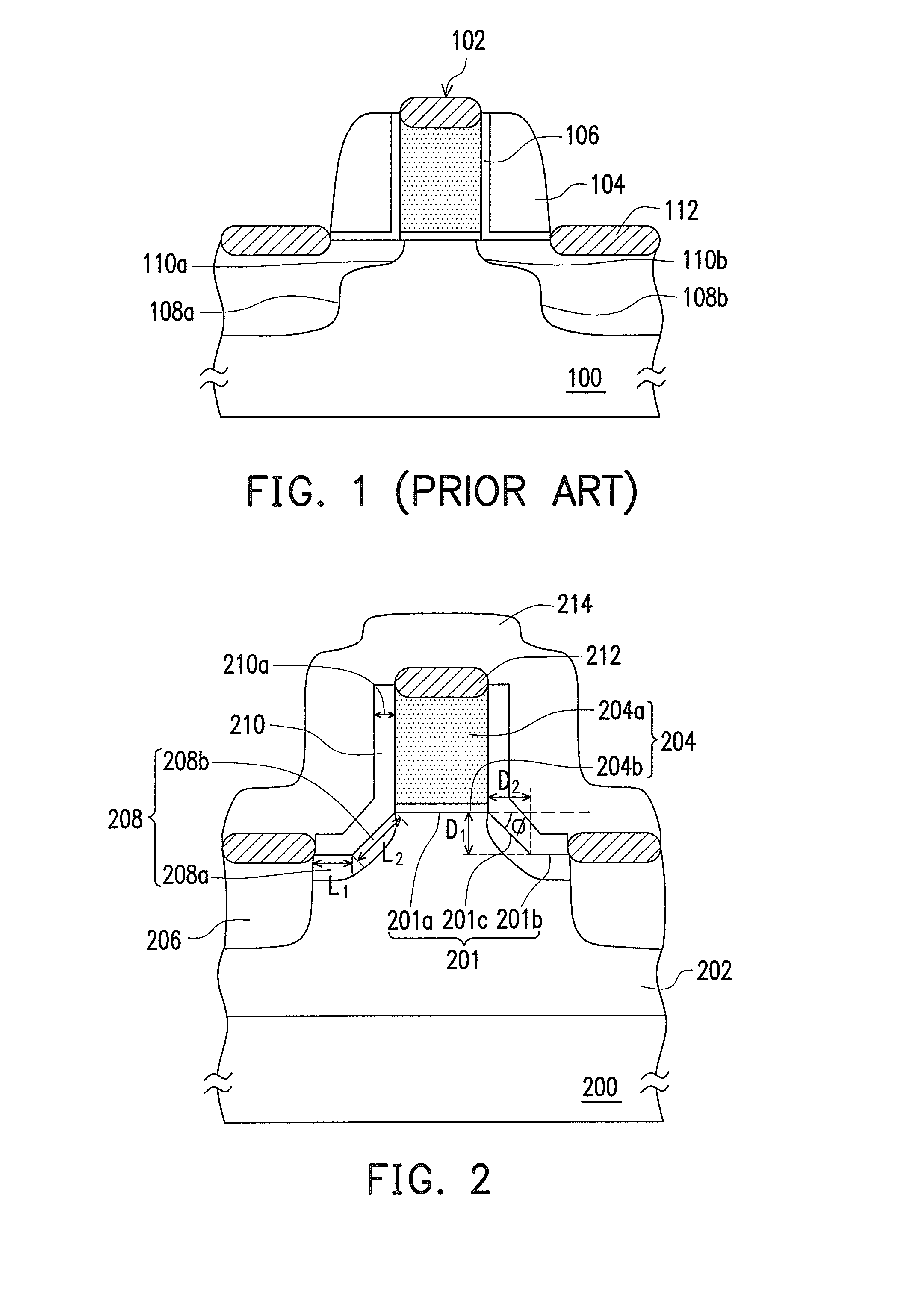
The heavily-doped source and drain extension regions 110a and 110b, however, results in higher gate-induced drain leakage (GIDL) current and severe hot carrier effect.

Method used


Image

  • Semiconductor device and method for fabricating the same
  • Semiconductor device and method for fabricating the same
  • Semiconductor device and method for fabricating the same

Examples


example

[0085]FIG. 6 schematically illustrates distribution curves of the lateral E-field versus various positions in the channel region parallel to the first surface according to the conventional NMOS and an example of the present invention.

[0086]As shown in FIG. 6, the lateral E-field at the channel region, which approaches to the interface of the gate structure and the silicon substrate, is simulated in the convention NMOS and the proposed NMOS of the present invention, respectively. The conventional NMOS and the NMOS of the present invention have the gates with same length, e.g. 90 nm. Under the same bias applied to the devices, the distribution of the lateral E-field in the conventional NMOS is much higher than that of the NMOS of the present invention. Since the lateral E-field affects hot carrier effect greatly, the conventional NMOS with the higher lateral E-field suffers from severe hot carrier effect, thereby degrading the performance of the device. Accordingly, the lateral E-fiel...


PUM


Abstract

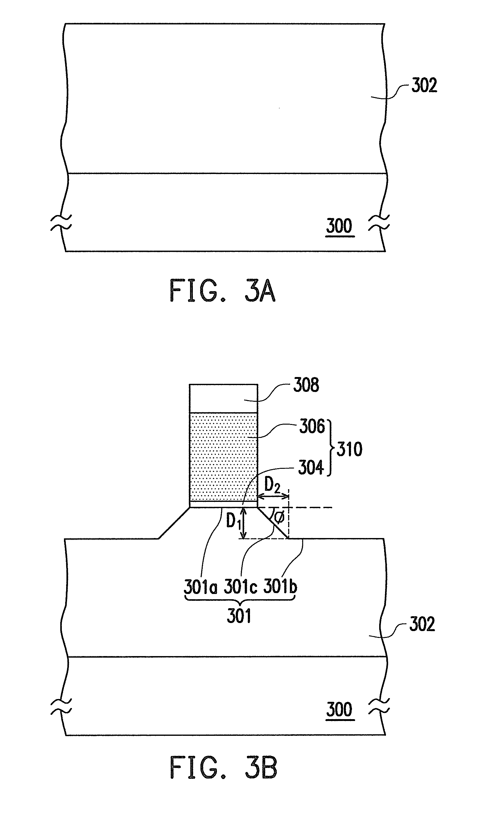
A semiconductor device is described, which includes a substrate, a gate structure, doped regions and lightly doped regions. The substrate has a stepped upper surface, which includes a first surface, a second surface and a third surface. The second surface is lower than the first surface. The third surface connects the first surface and the second surface. The gate structure is disposed on the first surface. The doped regions are configured in the substrate at both sides of the gate structure and under the second surface. The lightly doped regions are configured in the substrate between the gate structure and the doped regions, respectively. Each lightly doped region includes a first part and a second part connecting with each other. The first part is disposed under the second surface, and the second part is disposed under the third surface.

Description

BACKGROUND OF THE INVENTION[0001]1. Field of the Invention[0002]The present invention generally relates to a semiconductor device and a method for fabricating the same, and in particular, to a metal oxide semiconductor (MOS) transistor and the fabricating method thereof.[0003]2. Description of Related Art[0004]Along with rapid progress of semiconductor technology, the dimensions of semiconductor devices are reduced and the integrity thereof is promoted continuously to further advance the operating speed and performance of the integrated circuit. As the demand for device integrity is raised, dramatic changes in the device characteristics, e.g. current leakage, hot carrier effect and short channel effect (SCE), have to be considered so as to avoid a great impact on reliability and performance of the circuit.[0005]Taking a MOS transistor as an example, FIG. 1 is a schematic cross-sectional view illustrating a conventional MOS transistor. As shown in FIG. 1, a gate structure 102 is disp...

Claims


Application Information

Patent Timeline
Patent Type & Authority Patents(United States)
IPC IPC(8): H01L29/76H01L29/94
CPCH01L29/66636H01L29/7834H01L29/665
Inventor YANG, I-CHENWU, GUAN-WEICHANG, YAO-WENLU, TAO-CHENG
Owner MACRONIX INT CO LTD
Features
  • R&D
  • Intellectual Property
  • Life Sciences
  • Materials
  • Tech Scout
  • Unparalleled Data Quality
  • Higher Quality Content
  • 60% Fewer Hallucinations
Learn More