Liquid crystal display device and method for manufacturing the same

a liquid crystal display and display device technology, applied in the direction of liquid crystal compositions, instruments, chemistry apparatus and processes, etc., can solve the problems of difficult accurate positioning control, and achieve the effects of reducing cost, reducing expensive equipment, and high material-use efficiency

Active Publication Date: 2012-01-17
SEMICON ENERGY LAB CO LTD
View PDF17 Cites 15 Cited by
  • Summary
  • Abstract
  • Description
  • Claims
  • Application Information

AI Technical Summary

Benefits of technology

[0008]Accordingly, it is an object of the present invention to control the positioning of a spacer more accurately in a liquid crystal display device to prevent display defects due to incorrect positioning in a display region. It is another object of the present invention to provide a liquid crystal display device with higher image quality and reliability, and to provide a method for manufacturing the liquid crystal display device with high yield.
[0024]As a result, in a liquid crystal display device, the positioning of a spherical spacer can be controlled more accurately, display defects due to incorrect positioning in a display region can be prevented, and the space between substrates can be maintained uniformly. Furthermore, a liquid crystal display device with superior visibility and higher image quality and reliability can be manufactured with high yield.

Problems solved by technology

However, in the aforementioned ink jet method, the position of a spherical spacer cannot be controlled in a droplet discharged onto a substrate, and thus there are variations in the position where the spacer is discharged, which has made it difficult to accurately control the positioning.

Method used


Image

  • Liquid crystal display device and method for manufacturing the same
  • Liquid crystal display device and method for manufacturing the same
  • Liquid crystal display device and method for manufacturing the same

Examples


embodiment mode 1

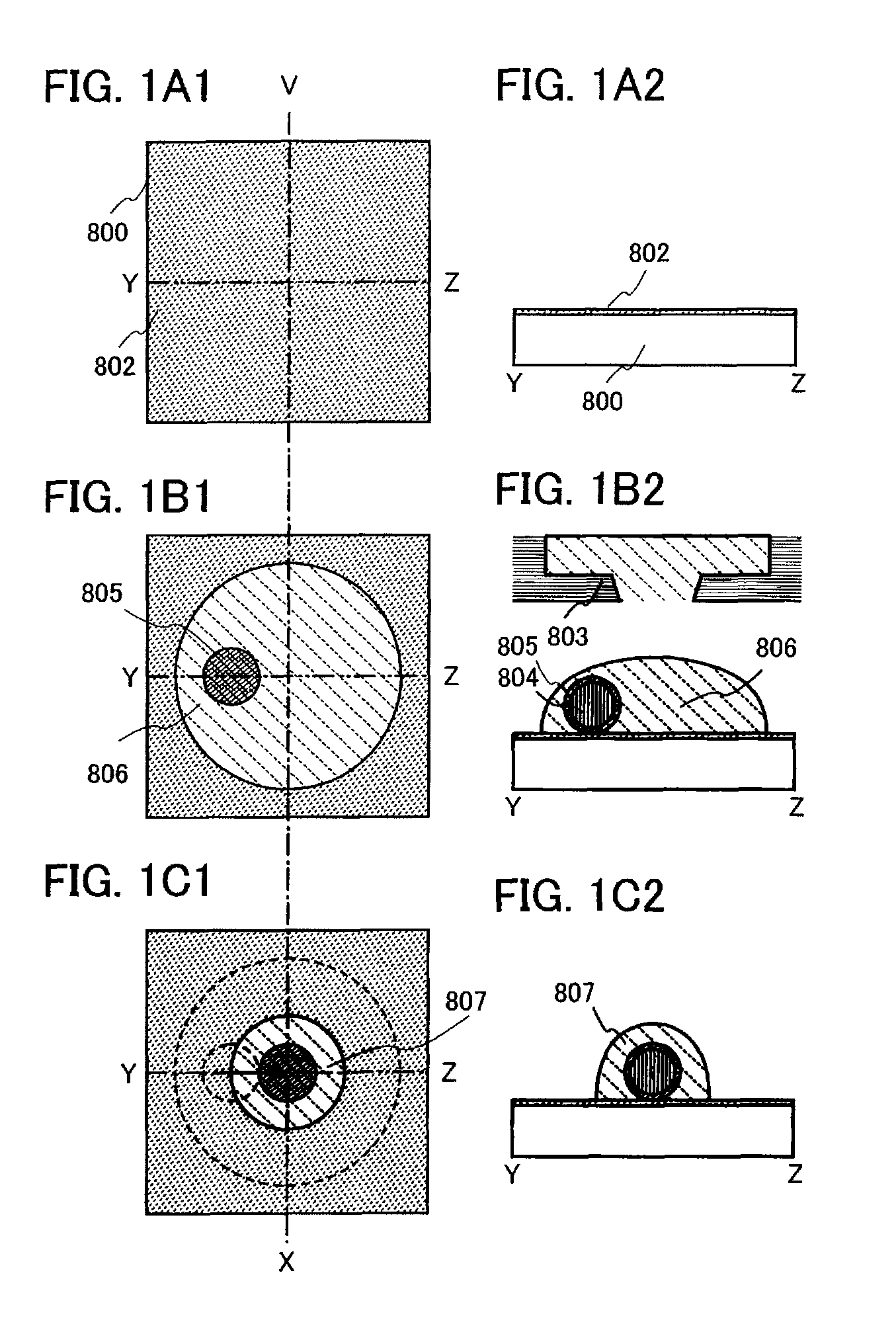
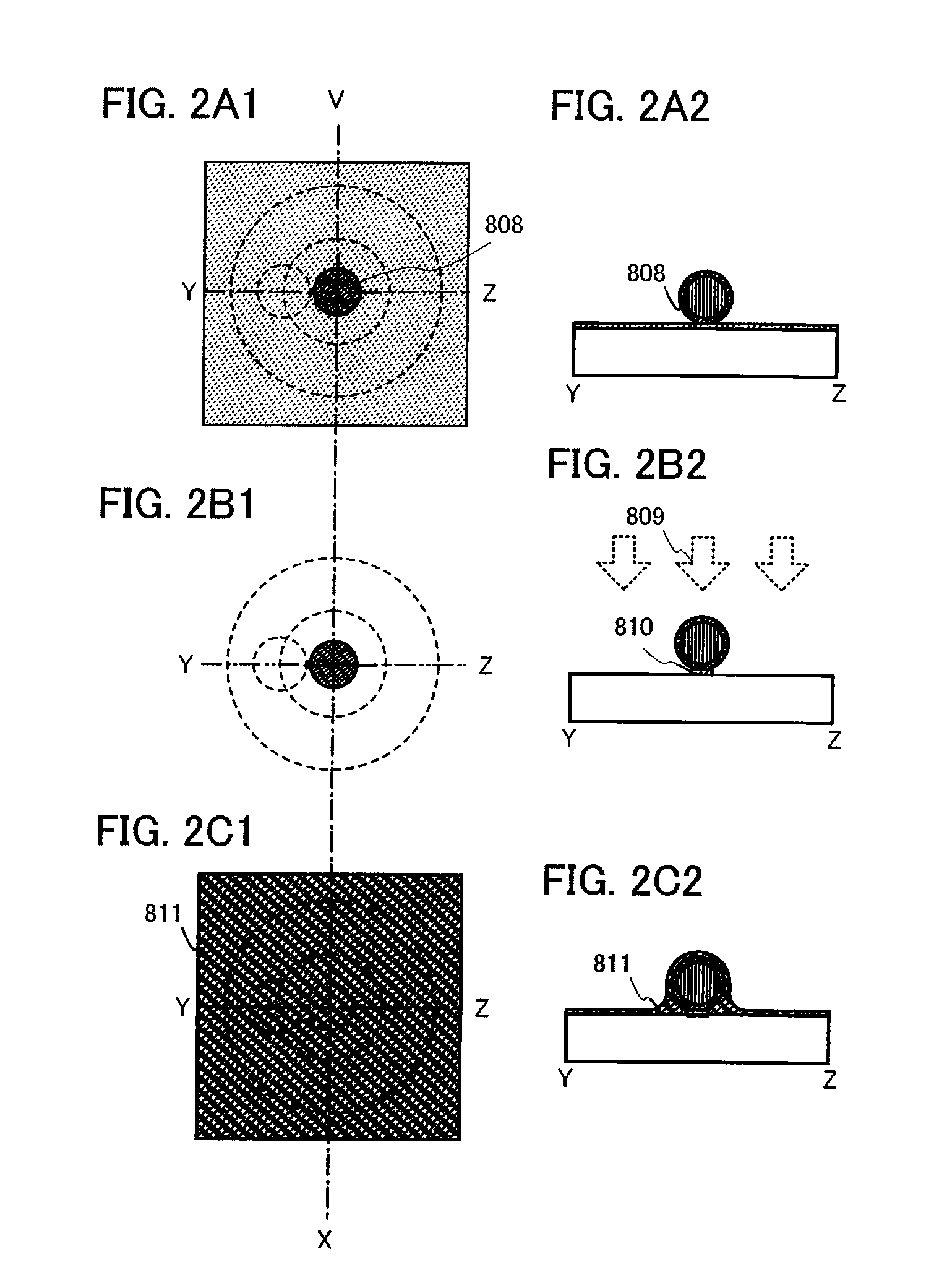
[0045]Described in this embodiment mode is an example of a liquid crystal display device that is improved in image quality and reliability and can be manufactured with high yield.

[0046]FIG. 3 illustrates a manufacturing process of a liquid crystal display device of the present invention. As illustrated in FIG. 3, in a method for manufacturing a liquid crystal display device, a spherical spacer is positioned over a substrate (or a conductive layer) by a droplet discharge method, an insulating layer functioning as an alignment film is formed thereover, rubbing treatment is performed, and then substrates are attached to each other. In the step of positioning the spherical spacer, first, an organosilane film having a hydrolytic group is formed as liquid-repellent treatment, and a liquid containing the spherical spacer attached with an adhesive is discharged by a droplet discharge method. As the liquid is dried, the spherical spacer moves toward the center of the liquid and the positioni...

embodiment mode 2

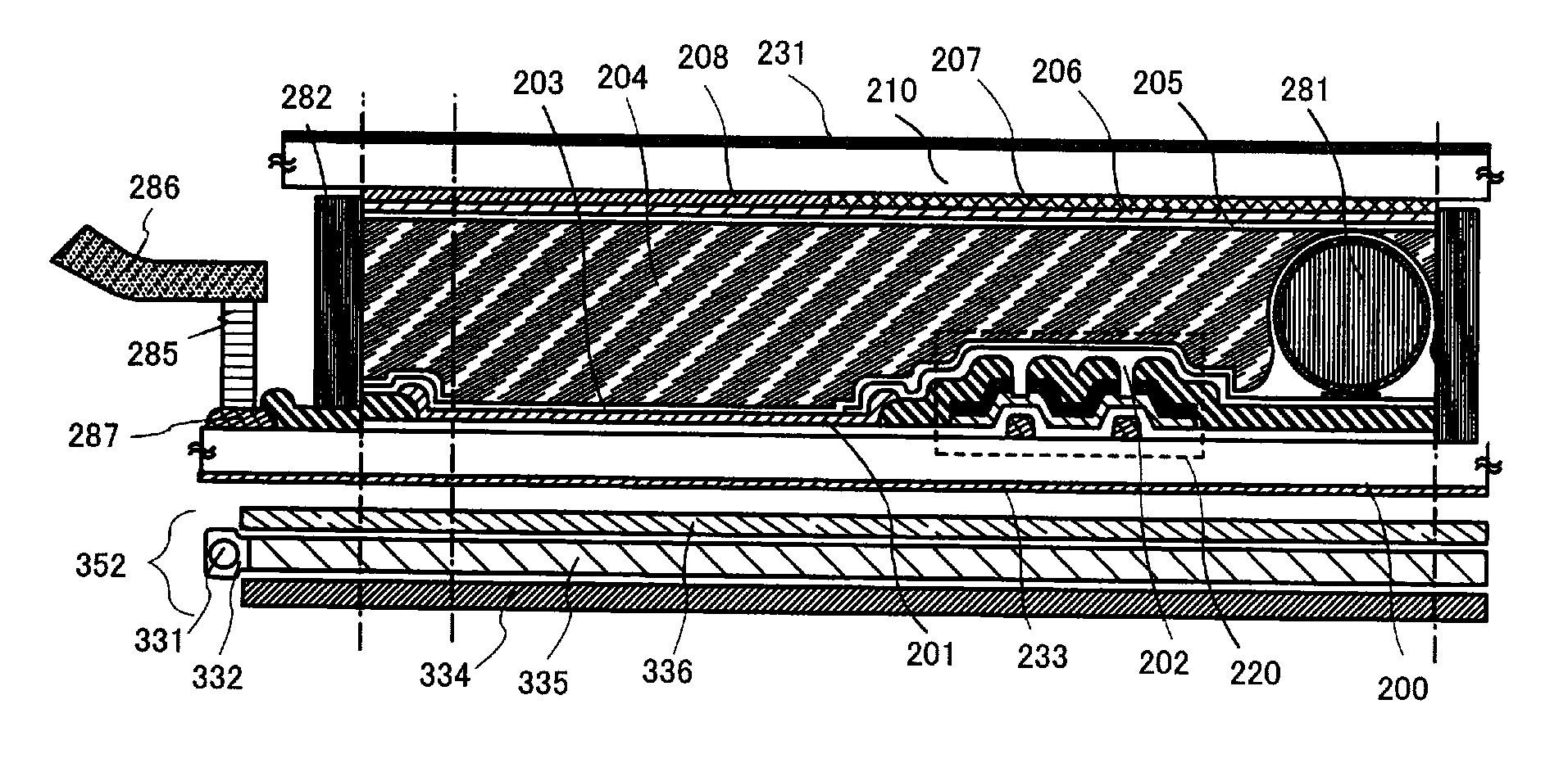
[0084]Described in this embodiment mode is an example of a liquid crystal display device that is improved in image quality and reliability and can be manufactured with high yield. More specifically, a passive matrix liquid crystal display device is described.

[0085]Description is made on a passive matrix liquid crystal display device of this embodiment mode to which the present invention is applied. FIG. 5A is a top view of the liquid crystal display device, and FIG. 5B is a cross-sectional view along line A-B of FIG. 5A. FIG. 5A includes, as illustrated in FIG. 5B, an insulating layer 1704 functioning as an alignment film, a coloring layer, a substrate 1710 that is a counter substrate, a polarizing plate 1714, and the like, although they are omitted and not illustrated in FIG. 5A.

[0086]In FIGS. 5A and 5B, a substrate 1700 is provided with pixel electrode layers 1701a, 1701b and 1701c that extend in a first direction, and an insulating layer 1712 functioning as an alignment film. The...

embodiment mode 3

[0109]Described in this embodiment mode is an example of a liquid crystal display device that is improved in image quality and reliability and can be manufactured with high yield. In this embodiment mode, a liquid crystal display device having a different structure from that of Embodiment Mode 2 is described. More specifically, an active matrix liquid crystal display device is described.

[0110]FIG. 6A is a top view of a liquid crystal display device and FIG. 6B is a cross-sectional view along line E-F of FIG. 6A. FIG. 6A includes, as illustrated in FIG. 6B, a liquid crystal layer and an alignment film, a counter electrode layer, a coloring layer, and the like that are provided on a counter substrate side, although they are omitted and not illustrated in FIG. 6A.

[0111]A first wiring that extends in a first direction and a second wiring that extends in a second direction perpendicular to the first direction are provided in matrix over a substrate 520 provided with an insulating layer 5...


PUM

PropertyMeasurementUnit
temperatureaaaaaaaaaa

Abstract

To control the positioning of a spacer more accurately in a liquid crystal display device to prevent display defects due to incorrect positioning in a display region. To provide a liquid crystal display device with higher image quality and reliability, and to provide a method for manufacturing the liquid crystal display device with high yield. In a liquid crystal display device, a region onto which a spherical spacer is discharged is subjected to liquid-repellent treatment in order to reduce the wettability with respect to a liquid in which the spherical spacer is dispersed. The liquid (the droplet) does not spread over the liquid-repellent region and is dried while moving the spherical spacer toward the center of the liquid. Thus, incorrect positioning shortly after discharging, which has been caused by the loss of control in the liquid, can be corrected by moving the spherical spacer while drying the liquid.

Description

BACKGROUND OF THE INVENTION[0001]1. Field of the Invention[0002]The present invention relates to a method for manufacturing a liquid crystal display device including a spacer.[0003]2. Description of the Related Art[0004]In a liquid crystal display device, in order to maintain the space (the gap) between substrates and control the thickness of a liquid crystal layer (cell gap), a columnar or spherical (bead) spacer is used.[0005]Typically, a columnar spacer is formed in such a manner that a photosensitive resin is applied by spin coating or the like and processed into a columnar shape by a photolithography process. In that case, it is possible to control the position where a columnar spacer is formed in a liquid crystal display device, but it is difficult to uniformly control the thickness of the columnar spacer, which determines the thickness of a liquid crystal layer. In addition, the use of the photolithography process leads to low material-use efficiency, increased cost, and decr...

Claims


Application Information

Patent Timeline
Patent Type & Authority Patents(United States)
IPC IPC(8): G02F1/1333
CPCG02F1/13394G02F1/13392G02F2202/28G02F1/13G02F1/1339
Inventor TAKAHASHI, ERIKAFUJII, GENFUKAI, SHUJINISHI, TAKESHI
Owner SEMICON ENERGY LAB CO LTD
Why Eureka
Try Eureka