Grinding method for wafer having crystal orientation

a crystal orientation and grinding method technology, applied in the field of wafer grinding method, can solve the problems of possible chipping of the wafer, achieve the effect of preventing the generation of chipping, low die strength, and reducing grinding efficiency

Active Publication Date: 2012-01-24
DISCO CORP
View PDF9 Cites 2 Cited by
  • Summary
  • Abstract
  • Description
  • Claims
  • Application Information

AI Technical Summary

Benefits of technology

[0010]It is therefore an object of the present invention to provide a wafer grinding method which can grind a wafer without reducing a grinding efficiency, prevent the generation of a chip having a low die strength, and prevent the chipping of the wafer.
[0012]According to the wafer grinding method of the present invention, the back side of the wafer is ground in the first grinding step in such a manner that the chuck table holding the wafer is rotated and the grinding ring is also rotated at a position where the grinding ring is passed through the center of the wafer. By the first grinding step, the thickness of the wafer is reduced to a predetermined thickness, so that the wafer can be ground without reducing a grinding efficiency. Thereafter, the back side of the wafer is further ground in the second grinding step in such a manner that a saw mark is not formed in a direction where the die strength of a chip is prone to be reduced in relation to the mark indicating the crystal orientation of the wafer. Accordingly, a reduction in die strength of the chip obtained by dividing the wafer can be prevented. Further, in the second grinding step, the upper surface (back side) of the outer circumferential portion of the wafer is positioned directly below the locus of rotation of the grinding ring and the grinding ring is lowered to partially grind the back side of the wafer. Thereafter, the chuck table and the grinding ring are relatively moved in parallel to thereby entirely grind the back side of the wafer. Thus, the grinding ring is kept in contact with the wafer during the second grinding step, so that the grinding operation can be smoothly performed without giving a shock to the wafer.

Problems solved by technology

In the wafer grinding method disclosed in Japanese Patent Laid-open No. 2005-28550 mentioned above, the outer circumferential surface of the wafer comes into impactive contact with the grinding wheel in the second grinding step, causing a possibility of chipping of the wafer.

Method used


Image

  • Grinding method for wafer having crystal orientation
  • Grinding method for wafer having crystal orientation
  • Grinding method for wafer having crystal orientation

Examples


Embodiment Construction

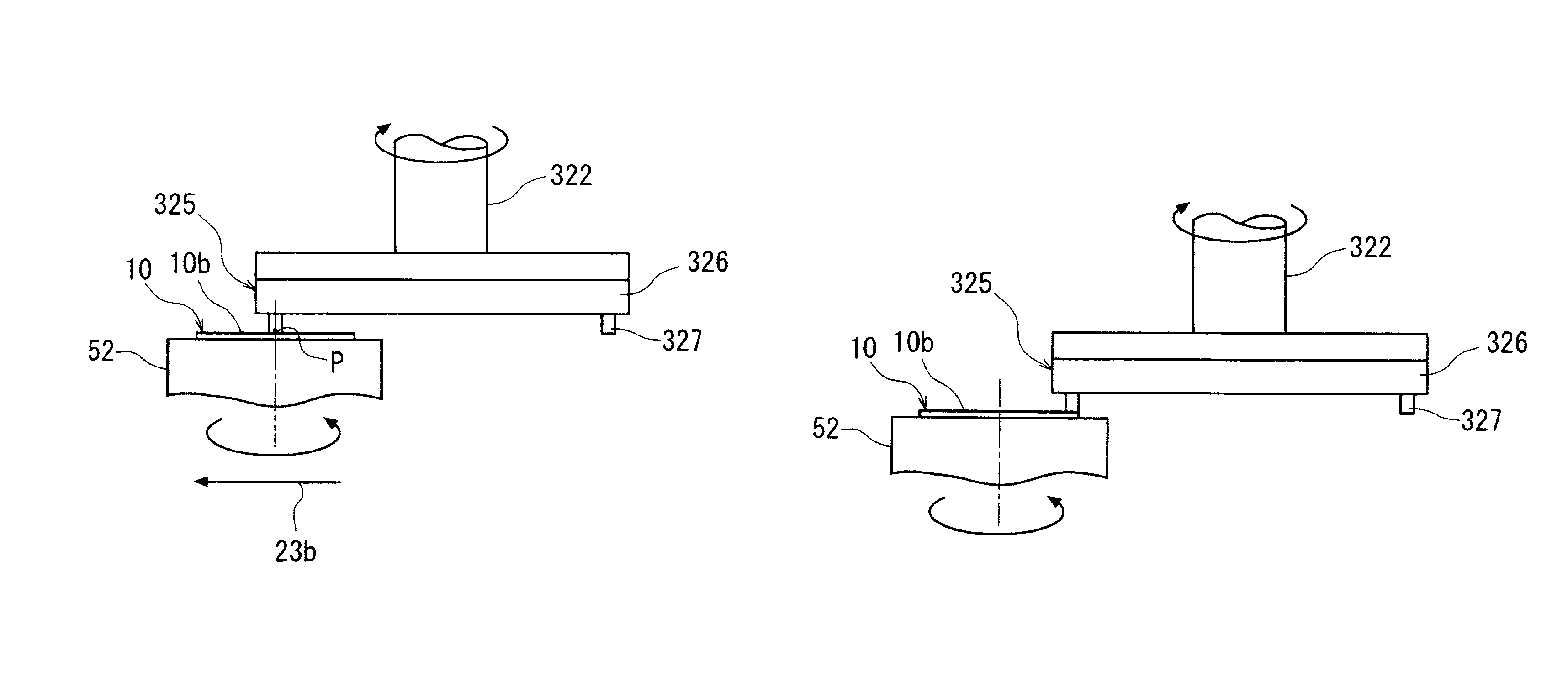
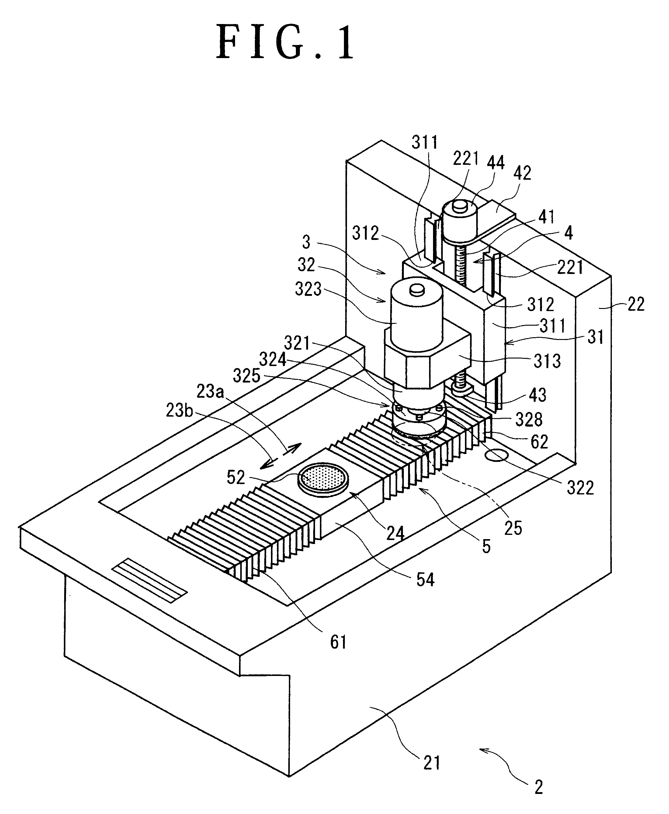
[0023]A preferred embodiment of the wafer grinding method according to the present invention will now be described in detail with reference to the attached drawings. FIG. 1 shows a perspective view of a grinding apparatus for carrying out the grinding method according to the present invention. The grinding apparatus shown in FIG. 1 includes an apparatus housing 2 generally designated. The apparatus housing 2 has a main portion 21 having a substantially rectangular parallelepiped shape extending in a horizontal direction and a vertical wall 22 provided at the rear end of the main portion 21 (right upper end as viewed in FIG. 1) so as to extend in a substantially vertical direction. A pair of parallel guide rails 221 are provided on the front surface of the vertical wall 22 so as to extend in the vertical direction. A grinding unit 3 as grinding means is mounted on the guide rails 221 so as to be movable in the vertical direction.

[0024]The grinding unit 3 includes a moving base 31 and...


PUM

PropertyMeasurementUnit
thicknessaaaaaaaaaa
feed speedaaaaaaaaaa
crystal orientationaaaaaaaaaa

Abstract

A grinding method for a wafer having a mark indicating the crystal orientation. The grinding method includes a first grinding step for grinding the upper surface of the wafer by rotating a chuck table holding the wafer thereon, rotating a grinding ring, positioning the grinding ring so that the grinding ring is passed through the center of the wafer, and feeding the grinding ring in a direction perpendicular to the chuck table; a wafer positioning step for positioning the upper surface of an outer circumferential portion of the wafer directly below the locus of rotation of the grinding ring; and a second grinding step for grinding the upper surface of the wafer by first stopping the rotation of the chuck table so that the mark indicating the crystal orientation of the wafer held on the chuck table is pointed in a predetermined direction, next feeding the grinding ring in the direction perpendicular to the chuck table, and next relatively moving the chuck table and the grinding ring in parallel.

Description

BACKGROUND OF THE INVENTION[0001]1. Field of the Invention[0002]The present invention relates to a wafer grinding method for grinding a wafer having crystal orientation.[0003]2. Description of the Related Art[0004]In a semiconductor device fabrication process, a plurality of crossing division lines called streets are formed on the front side of a substantially disk-shaped semiconductor wafer to thereby partition a plurality of rectangular regions where devices such as ICs and LSIs are respectively formed. The semiconductor wafer having many devices as mentioned above is divided along these streets to thereby obtain individual semiconductor chips. Also in the case of a wafer composed of a substrate of lithium tantalate, for example, and a plurality of piezoelectric elements provided in the substrate, the wafer is cut along predetermined streets to obtain individual chips, which are widely used in electrical equipment.[0005]To reduce the size and weight of each chip, the back side of ...

Claims


Application Information

Patent Timeline
Patent Type & Authority Patents(United States)
IPC IPC(8): B24B1/00
CPCB24B7/228
Inventor MASUDA, TAKATOSHI
Owner DISCO CORP
Why Eureka
Try Eureka