Defect detecting apparatus and method

a technology of defect detection and detection apparatus, applied in the field of defect detection apparatus and method, can solve the problems of not being able to enter the imaging surface of solid-state imaging element, subjecting the cover glass thereof to defect inspection, scattered or blocked parts of the subject light, etc., and achieve the effect of ensuring the detection of defects

Inactive Publication Date: 2012-01-31
FUJIFILM CORP
View PDF4 Cites 5 Cited by
  • Summary
  • Abstract
  • Description
  • Claims
  • Application Information

AI Technical Summary

Benefits of technology

[0006]In view of the above, an object of the present invention is to provide a defect detecting apparatus and method for surely detecting defects without performing unnecessary inspection.
[0008]The eliminating device includes: a defect candidate image identifying device for identifying a defect candidate image containing an image of the defect and the blurred image in the composite image; and a blurred image eliminating device for eliminating the blurred image from the defect candidate image.
[0012]A defect detecting method of the present invention includes the steps of: focusing and imaging each surface to be inspected; combining images of the surfaces obtained by the imaging step so as to create a composite image; eliminating at least one blurred image from the composite image, the blurred image being caused by a defect which resides on one of the surfaces and appears on the other of the surfaces; and detecting the defect based on the composite image from which the blurred image is eliminated.
[0017]According to the present invention, it is possible to surely detect defects without performing unnecessary inspection by eliminating a blurred image from a composite image obtained by combining images of the respective surfaces to be inspected.

Problems solved by technology

When the cover glass has defects such as stain, scratch, and incorporation of foreign materials, a part of the subject light is scattered or blocked by these defects, and not able to enter the imaging surface of the solid state imaging element.
Therefore, before the solid state imaging device is mounted to the electric camera, the cover glass thereof is subjected to defect inspection.
However, when the front and rear side surfaces of the cover glass are focused and captured respectively, if the depth of field is shallow, the following problems may occur.
As a result, unnecessary inspection is performed, and thereby the productivity is decreased.

Method used


Image

  • Defect detecting apparatus and method
  • Defect detecting apparatus and method
  • Defect detecting apparatus and method

Examples


first embodiment

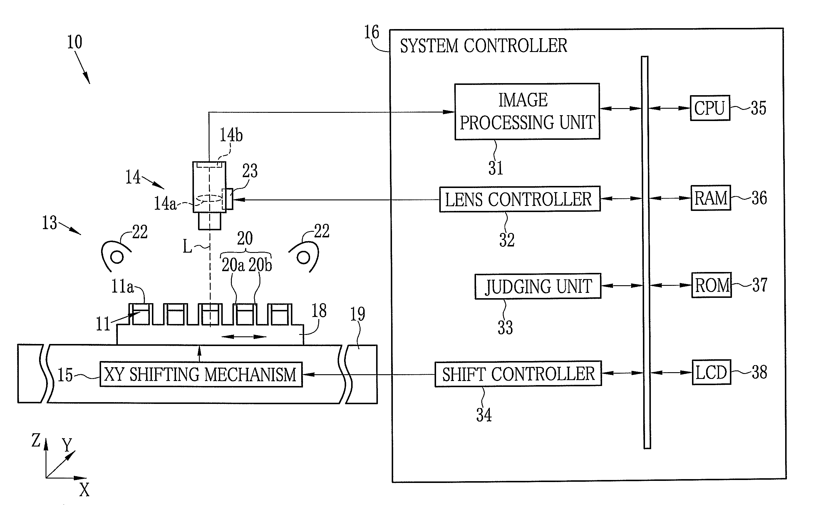
[0029]As shown in FIG. 1, a defect detecting apparatus 10 detects defects on a cover glass 11a of a solid state imaging device 11. The defects on the cover glass 11a include a spot defect (defect caused by incorporation of foreign materials to have roughness on the surface), a scratch defect, a stain defect, and the like.

[0030]The defect detecting apparatus 10 includes an inspection stage 13, a camera 14, an XY shifting mechanism 15, and a system controller 16. The inspection stage 13 includes a jig 18 and a base 19. The jig 18 is movable on the base 19 in X and Y directions. A plurality of clamps 20 are disposed on an upper surface of the jig 18 in a matrix fashion in the X and Y directions. Each of the clamps 20 includes a pair of pins 20a and 20b. The pair of pins 20a and 20b holds the solid state imaging device 11 horizontally such that the cover glass 11a faces upward. Further, above both right and left sides of the jig 18, a light source 22 is respectively disposed. Light from...

second embodiment

[0053]In a second embodiment of the present invention, there is described defect judgment in a case where one defect candidate image includes two or more kinds of defect images and the blurred images thereof overlapped with each other. Note that except the processing in the image processing unit, the second embodiment is identical to the first embodiment, and therefore its detailed description will be omitted.

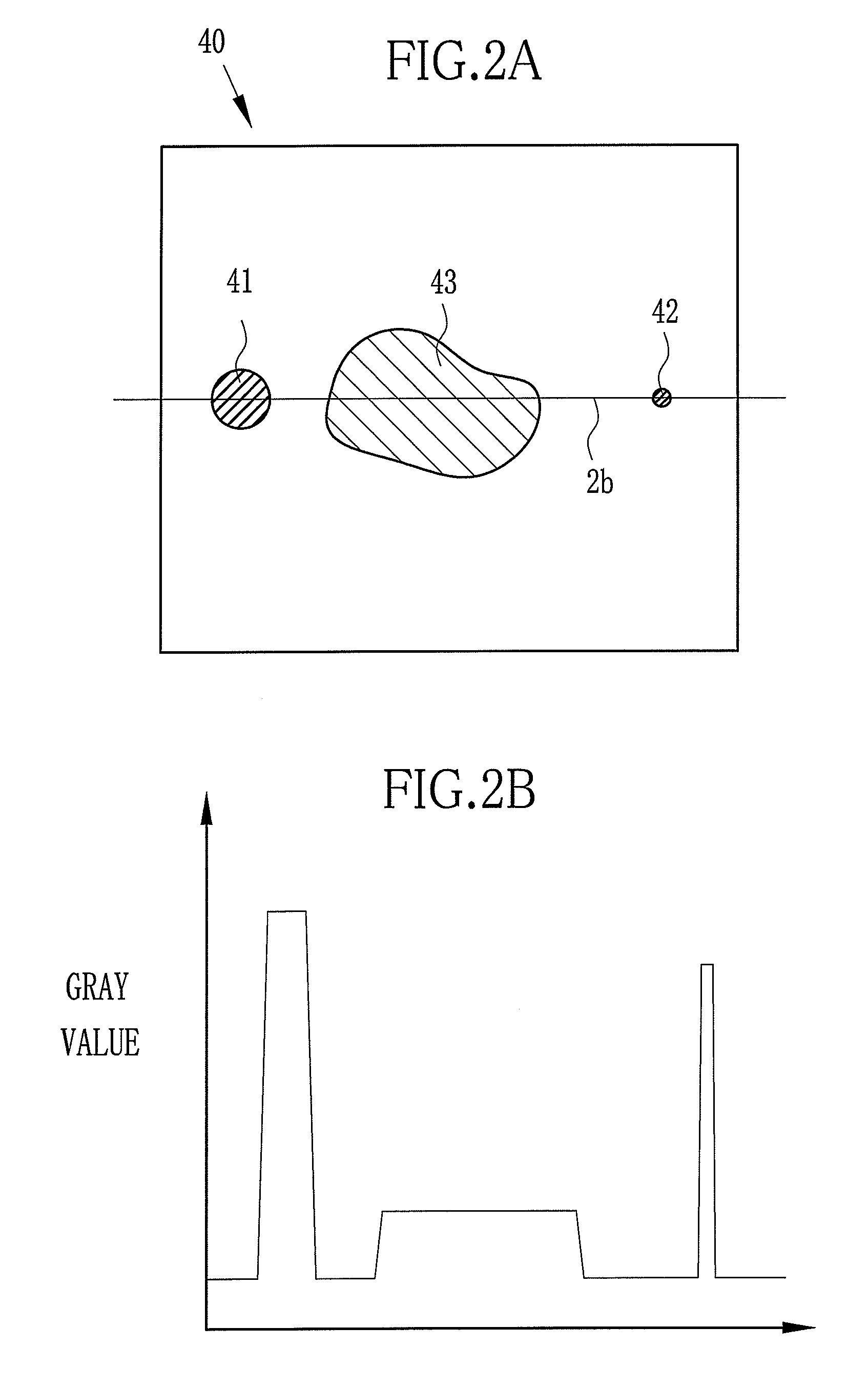
[0054]As in the case of the image processing unit 31 of the first embodiment, in the image processing unit 31, the front side image is created based on the front side imaging signal, and the rear side image is created based on the rear side imaging signal, the signals being respectively sent from the camera 14. As shown in FIG. 6A, in a front side image 70, there are recorded the spot defect image 71, and a blurred image 72 caused by the stain defect on the rear side surface of the cover glass 11a. The spot defect image 71 and the blurred image 72 are overlapped with each other...


PUM


Abstract

A front side surface of a cover glass of a solid state imaging device is focused, and a front side image is captured. Next, a rear side surface of the cover glass is focused, and a rear side image is captured. The front side image and the rear side image are combined with each other to create a composite image. A first threshold value is set for each pixel in the composite image by dynamic thresholding. An image composed of pixels whose gray values exceed the first threshold value is identified as a defect candidate image. The maximum gray value of the defect candidate image is multiplied by a constant rate to set a second threshold value. An image composed of pixels whose gray value is less than the second threshold value is eliminated as a blurred image from the defect candidate image.

Description

FIELD OF THE INVENTION[0001]The present invention relates to a defect detecting apparatus and method for detecting defects of a transparent member such as a cover glass of a solid state imaging device.BACKGROUND OF THE INVENTION[0002]An electronic camera such as a digital camera incorporates a solid state imaging device for photoelectrically converting subject light into an electric signal. The solid state imaging device includes a solid state imaging element such as a charge-coupled device (CCD) and a complementary metal-oxide semiconductor (CMOS), a package for housing the solid state imaging element (bare chip), and a cover glass attached to the package for covering an imaging surface of the solid state imaging element.[0003]When the cover glass has defects such as stain, scratch, and incorporation of foreign materials, a part of the subject light is scattered or blocked by these defects, and not able to enter the imaging surface of the solid state imaging element. Therefore, bef...

Claims


Application Information

Patent Timeline
Patent Type & Authority Patents(United States)
IPC IPC(8): G06K9/00
CPCG06K9/00G06T7/0004H04N5/2171G06V10/273G06V2201/06H04N23/811G06F18/00
Inventor ONODA, YUJI
Owner FUJIFILM CORP
Why Eureka
Try Eureka