Digital data architecture employing redundant links in a daisy chain of component modules

a technology of digital data and component modules, applied in the direction of memory adressing/allocation/relocation, instruments, error detection/correction, etc., can solve the problems of path consumption, memory subsystem and speed at which it operates, inability to perform useful work, etc., to reduce the average traffic on each link, reduce latency, and increase access efficiency

Active Publication Date: 2012-01-31
LENOVO GLOBAL TECH INT LTD
View PDF17 Cites 7 Cited by
  • Summary
  • Abstract
  • Description
  • Claims
  • Application Information

AI Technical Summary

Benefits of technology

[0012]In the preferred embodiment, the redundant paths or links are used in a non-degraded operating mode to provide higher bandwidth and / or reduced latency of data communications in the daisy chain. Failure of a single module or link in the daisy chain may reduce bandwidth and / or increase latency, but the data connection will still be maintained.
[0014]By configuring modules, and particularly memory chip modules, in daisy chains having multiple redundant paths as disclosed herein, access to the downstream modules in a daisy chain is maintained notwithstanding the failure of any single module in the chain. Furthermore, in the absence of a module failure, the redundant paths can be used to increase the efficiency of access, either by reducing latency time to reach a module far down the chain, or by reducing the average traffic on each link in the chain.

Problems solved by technology

In operation, the processor is constantly accessing instructions and other data in memory, without which it is unable to perform useful work.
The design of the memory subsystem and speed at which it operates are critical issues in the overall performance of any computer system.
As computers have grown more complex, this path has consumed a larger share of the access time.
In these systems, it is simply not possible for direct paths to exist from every processor to every memory module.
This complexity not only affects access time, but the reliability of the memory subsystem as well.
As the number of processors and size of memory grows, these issues become more acute.
However, there are certain limitations to this arrangement.
The time to access a memory module increases in accordance with its position in the daisy chain, which places practical limitations on the length of the daisy chain.

Method used


Image

  • Digital data architecture employing redundant links in a daisy chain of component modules
  • Digital data architecture employing redundant links in a daisy chain of component modules
  • Digital data architecture employing redundant links in a daisy chain of component modules

Examples


Embodiment Construction

Future Memory Chip Overview

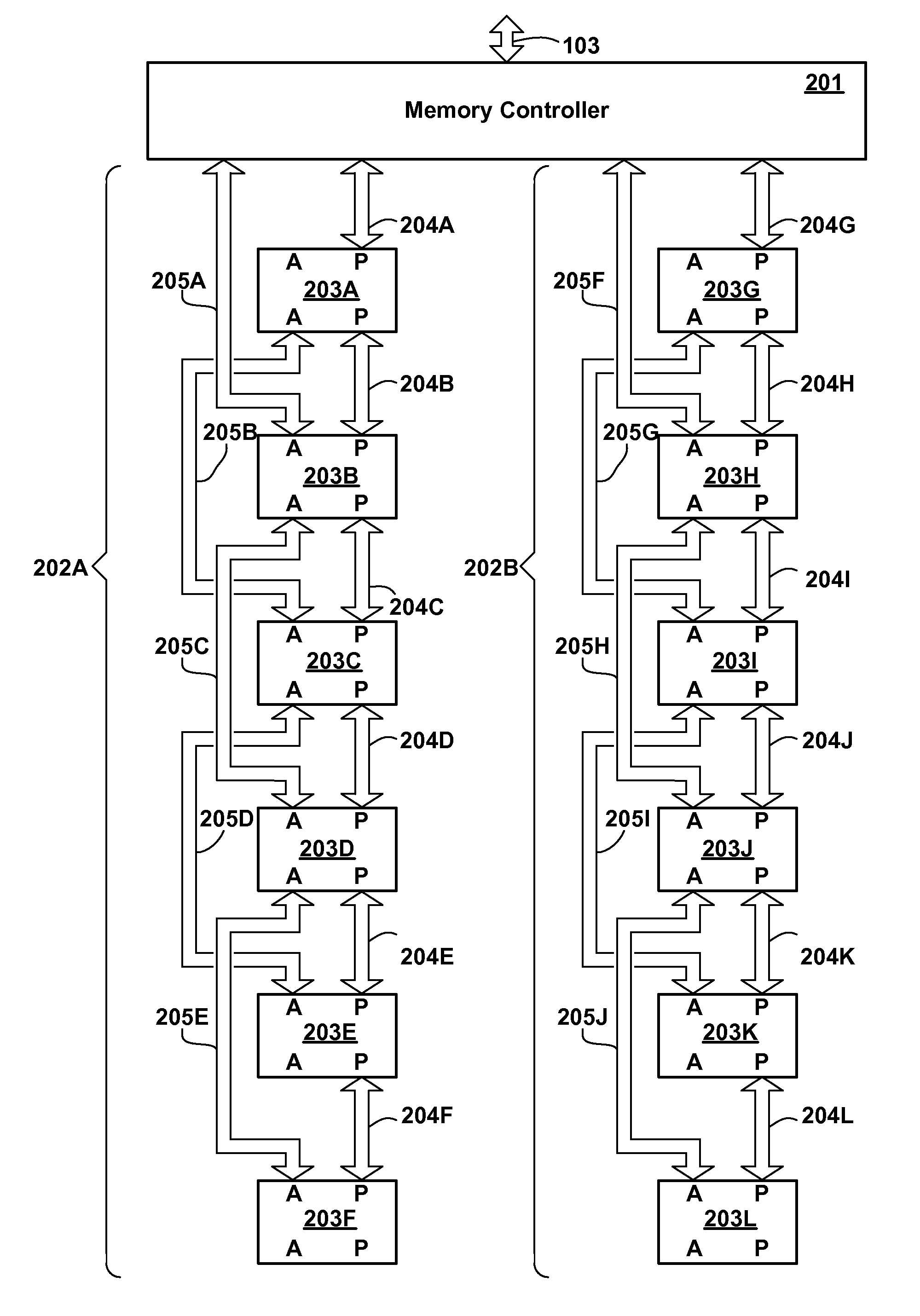
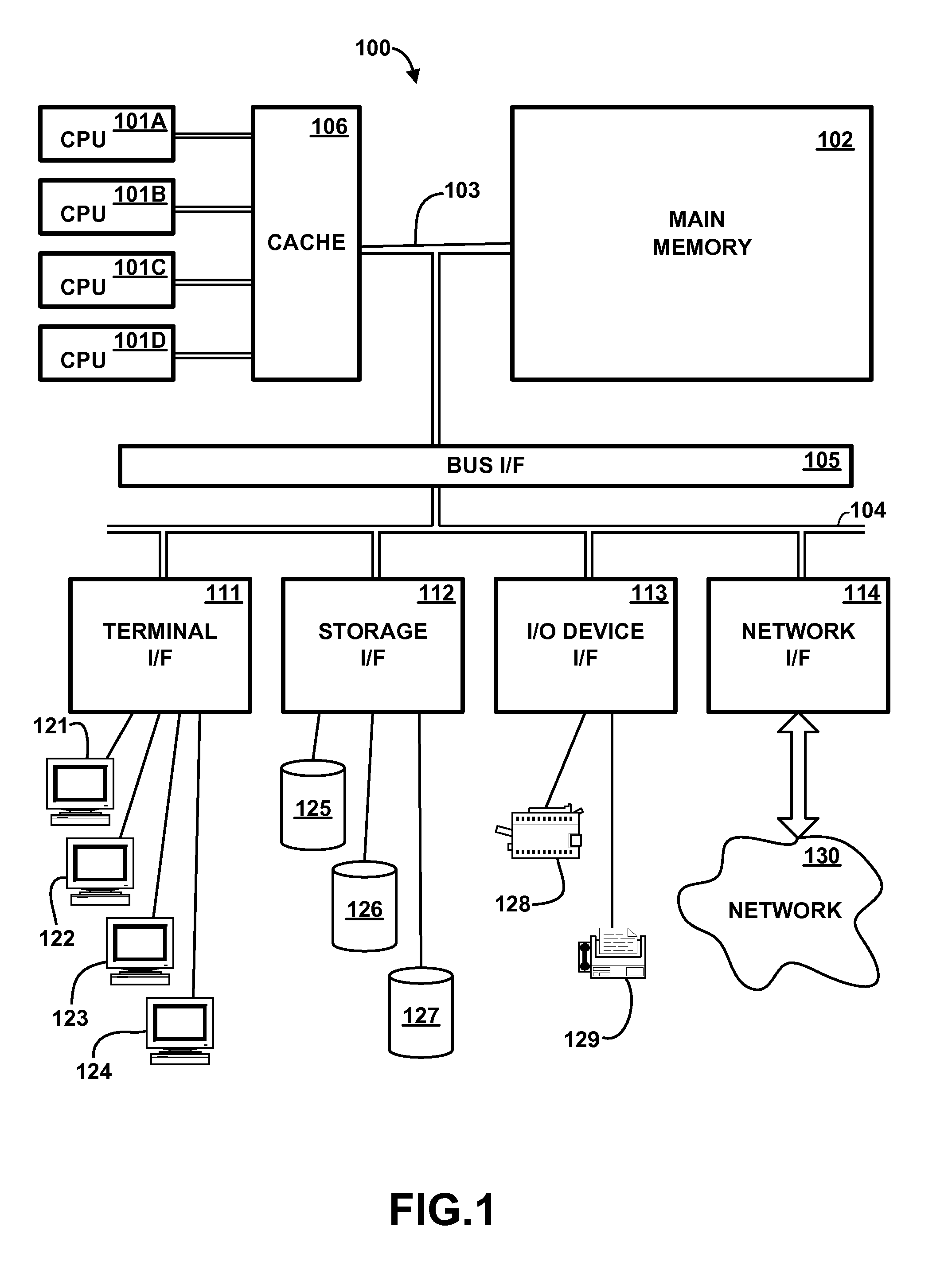
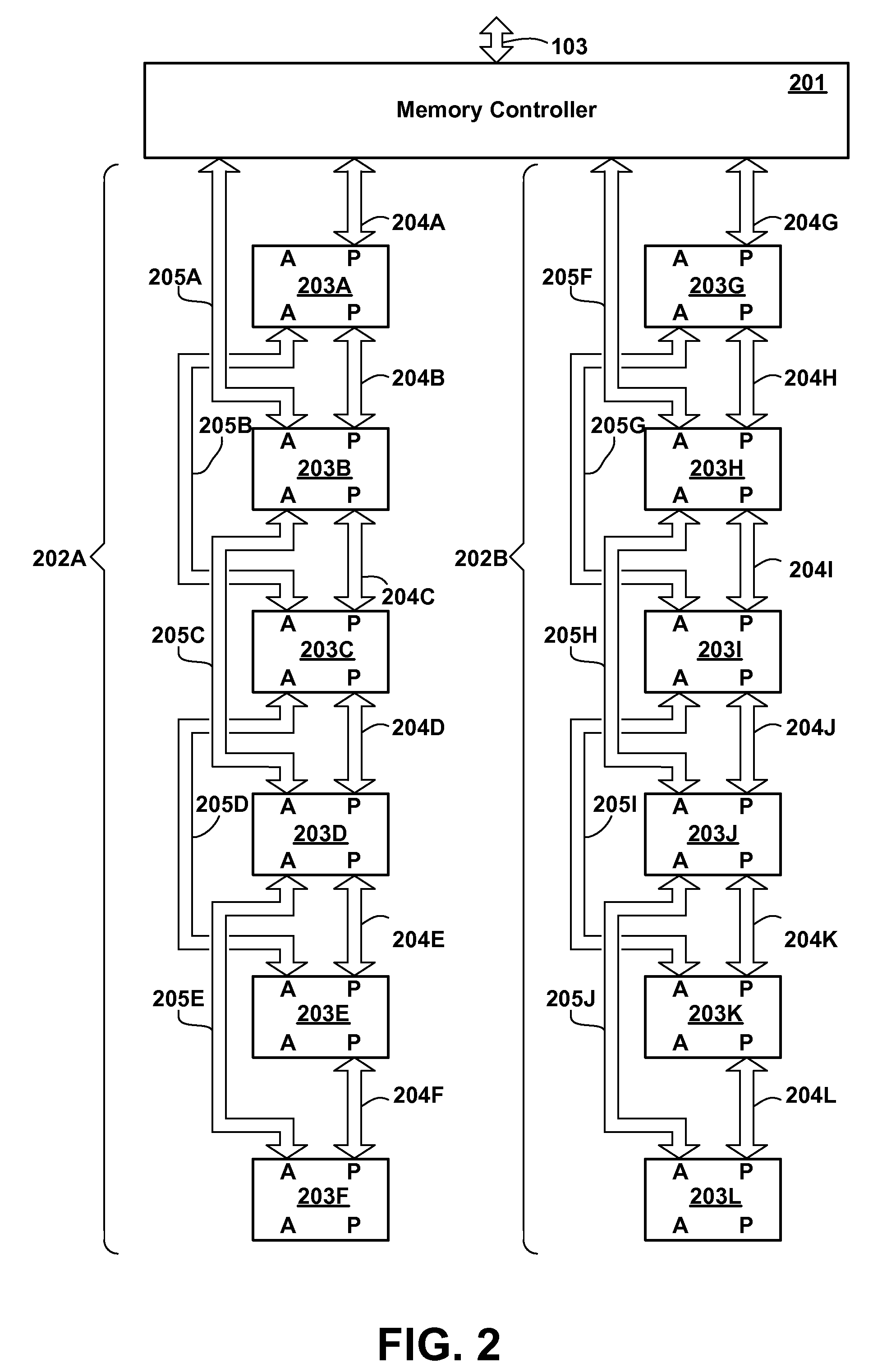
[0027]The present inventors envision a buffered memory chip module and memory chip architecture supporting chains of memory chips. Such an architecture is described in the following U.S. patents and commonly assigned copending patent applications, each of which is herein incorporated by reference: U.S. Pat. No. 7,345,900 to Bartley et al., issued Mar. 18, 2008; U.S. application Ser. No. 11 / 459,957, filed Jul. 26, 2006, entitled “Memory System Having Self Timed Daisy Chained Memory Chips”; U.S. application Ser. No. 11 / 459,969, filed Jul. 26, 2006, entitled “Carrier Having Daisy Chained Memory Chips”; U.S. application Ser. No. 11 / 459,983, filed Jul. 26, 2006, entitled “Carrier Having Daisy Chain of Self Timed Memory Chips”; U.S. Pat. No. 7,342,816 to Bartley et al., issued Mar. 11, 2008; U.S. application Ser. No. 11 / 459,997, filed Jul. 26, 2006, entitled “Daisy Chainable Self Timed Memory Chip”; U.S. application Ser. No. 11 / 459,974, filed Jul. 26, 2006, enti...


PUM


Abstract

A communications architecture utilizes modules arranged in a daisy-chain, each module supporting multiple input and output ports. Point-to-point links are arranged so that a first output link of each of multiple modules connects to the next module in the chain, and a second output link connects to a module after it, and inputs arranged similarly, so that any single module can be by-passed in the event of malfunction. Multiple chains may be cross-linked and / or serviced by hubs or chains of hubs. Preferably, the redundant links are used in a non-degraded operating mode to provide higher bandwidth and / or reduced latency of communication. The exemplary embodiment is a memory subsystem in which the modules are buffered memory chips.

Description

FIELD OF THE INVENTION[0001]The present invention relates to digital data processing hardware, and in particular to the design and operation of daisy-chained modules in a digital data processing system.BACKGROUND OF THE INVENTION[0002]In the latter half of the twentieth century, there began a phenomenon known as the information revolution. While the information revolution is a historical development broader in scope than any one event or machine, no single device has come to represent the information revolution more than the digital electronic computer. The development of computer systems has surely been a revolution. Each year, computer systems grow faster, store more data, and provide more applications to their users.[0003]A modern computer system typically comprises one or more central processing units (CPUs) and supporting hardware necessary to store, retrieve and transfer information, such as communications buses and memory. It also includes hardware necessary to communicate wi...

Claims


Application Information

Patent Timeline
Patent Type & Authority Patents(United States)
IPC IPC(8): G06F12/16G06F11/00
CPCG06F11/201G06F13/1684G11C5/06
Inventor BARTLEY, GERALD KEITHBECKER, DARRYL JOHNBORKENHAGEN, JOHN MICHAELGERMANN, PHILIP RAYMONDHOVIS, WILLIAM PAULMAXSON, MARK OWEN
Owner LENOVO GLOBAL TECH INT LTD
Why Eureka
Try Eureka