Film forming method, film forming apparatus and storage medium

a film forming and film technology, applied in the direction of chemical vapor deposition coating, semiconductor/solid-state device details, coatings, etc., can solve the problems of copper line formation defect, abnormal growth, and reduction in production yield, and achieve excellent adhesiveness to the base film

Inactive Publication Date: 2012-03-06
TOKYO ELECTRON LTD
View PDF13 Cites 3 Cited by
  • Summary
  • Abstract
  • Description
  • Claims
  • Application Information

AI Technical Summary

Benefits of technology

[0009]The present invention is devised in view of the above-mentioned problems. An object of the present invention is to provide a film forming method and a film forming apparatus capable of obtaining a copper film having excellent adhesiveness to a base film by preventing the formation of an organic impurity layer and the abnormal growth of the copper film.
[0011]In accordance with the first aspect of the present invention, since the adhesion layer is formed under an atmosphere containing water vapor, although the base film on which the adhesion layer is formed is made of metal such as titanium having a high oxidation tendency, it is possible to prevent formation of the organic impurity layer and improve adhesiveness between the base film and the adhesion layer. Further, the processing chamber is evacuated after formation of the adhesion layer and, then, the Cu(hfac)TMVS gas is resupplied to form the copper film, thereby suppressing an abnormal growth of the copper film due to the water vapor.
[0013]In accordance with the second aspect of the present invention, since the adhesion layer is formed under an atmosphere containing water vapor, although the base film on which the adhesion layer is formed is made of metal such as titanium having a high oxidation tendency, it is possible to prevent formation of the organic impurity layer and improve adhesiveness between the base film and the adhesion layer. Further, the processing chamber is evacuated after formation of the adhesion layer and, then, the Cu(hfac)TMVS gas and a small amount of water vapor are resupplied to form the copper film, thereby suppressing an abnormal growth of the copper film due to the water vapor.

Problems solved by technology

Accordingly, electrical characteristics deteriorate or the copper film is peeled off while processing the wafer, resulting in a reduction in production yield.
Further, since the organic impurity layer has poorer wettability than the base film, copper can be easily aggregated to thereby reduce buriability of the copper in a trench having a high aspect ratio, thereby causing a formation defect of the copper line.
However, in the CVD using Cu(hfac)TMVS as a material, it is known that the water vapor causes a demerit of abnormal growth of the copper film in a needle shape though it prevents formation of the organic impurity layer.
From this point, in the technology disclosed in the above-mentioned document, since the water vapor still remains in the processing chamber even though the supplies of these gases are stopped, it is difficult to immediately stop the abnormal growth of the copper film.
In this case, since a gap develops between the base film and the copper film, it is difficult to improve adhesiveness.

Method used


Image

  • Film forming method, film forming apparatus and storage medium
  • Film forming method, film forming apparatus and storage medium
  • Film forming method, film forming apparatus and storage medium

Examples


experiment 1

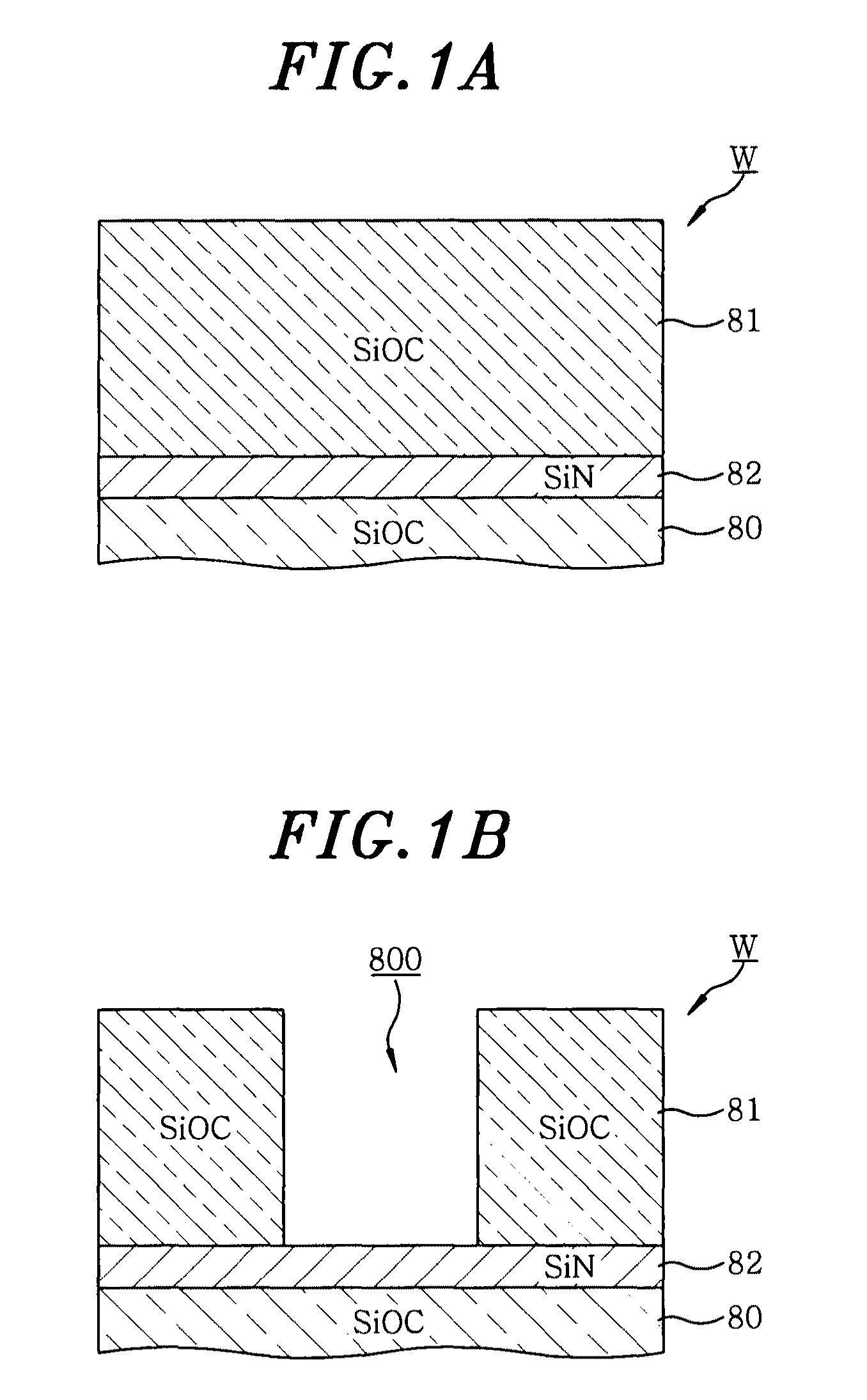
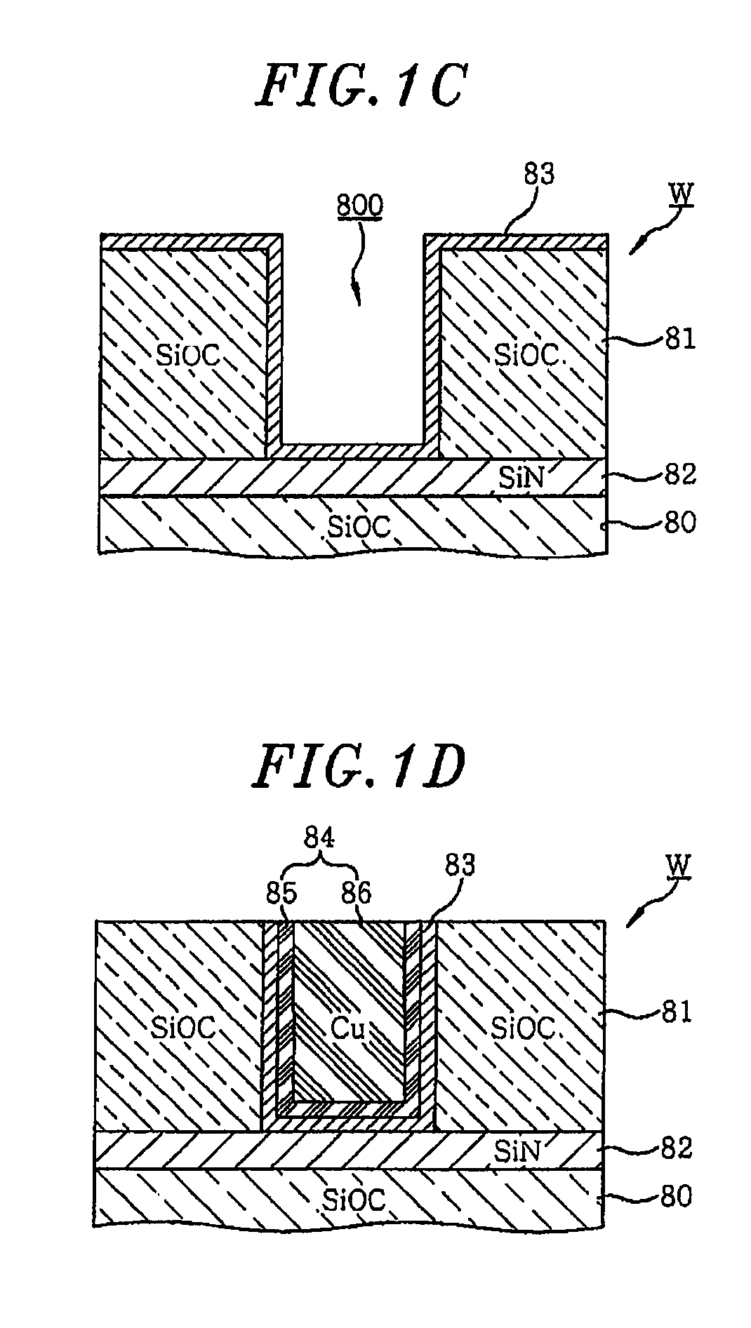
[0062]In accordance with the film forming method of the embodiment of the present invention, an adhesion layer and a copper film were formed on a base film made of titanium. Then, cross sections of the films were observed.

example 1-1

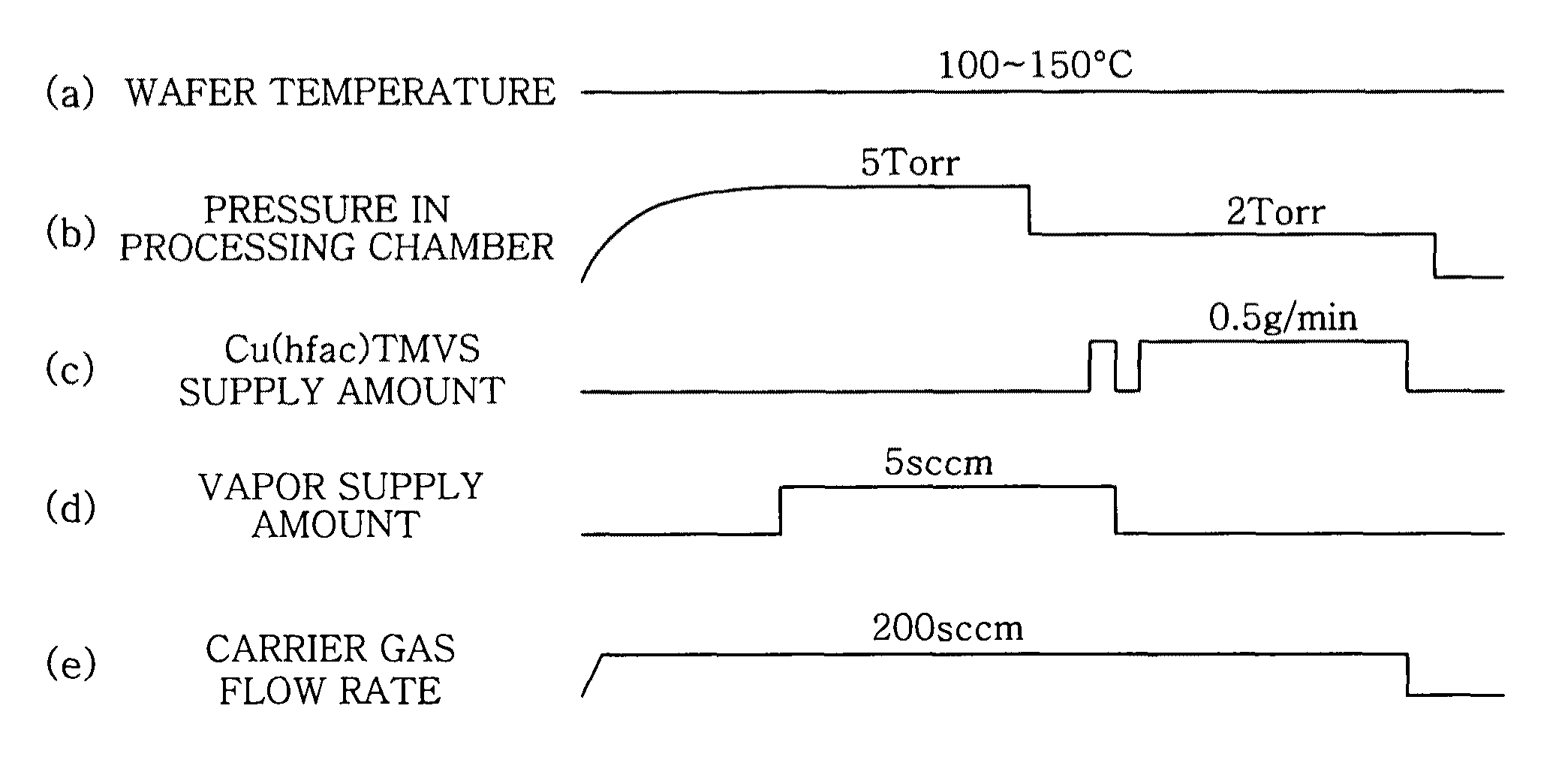
[0063]The copper film was formed on the surface of a barrier metal of titanium coated on the wafer W in accordance with the process sequence shown in FIG. 3. Further, the process temperature was maintained at 130° C. and the supply of water vapor was stopped during the period of time between the time T6 and the time T7. The cross sections of the obtained copper film and the base film were photographed by SEM and the result thereof is shown in FIG. 5A.

experiment 2

[0068]In accordance with the film forming method of the embodiment of the present invention, a copper film was formed. Then, the surface of the film was observed.


PUM

PropertyMeasurementUnit
temperatureaaaaaaaaaa
widthaaaaaaaaaa
widthaaaaaaaaaa

Abstract

A film forming method is provided with a substrate placing step wherein a substrate is placed in a process chamber in an airtight status; a first film forming step wherein the process chamber is supplied with water vapor and a material gas including an organic compound of copper, and an adhered layer of copper is formed on the substrate; an exhaust step wherein the water vapor and the material gas in the process chamber are exhausted; and a second film forming step wherein the process chamber is resupplied with only the material gas and a copper film is further formed on the adhered layer.

Description

FIELD OF THE INVENTION[0001]The present invention relates to a technology for forming a copper film on a substrate such as a semiconductor wafer by using an organic compound of copper as a material.BACKGROUND OF THE INVENTION[0002]In a recent wiring technology, copper lines are replacing aluminum lines to improve performance of a semiconductor device. In a manufacturing process of the semiconductor device, a technology for forming a copper film on a surface of a semiconductor wafer (hereinafter, referred to as a “wafer”) is important. A chemical vapor deposition method (hereinafter, referred to as “CVD”) using a copper organic compound as a material has been known as one of technologies for forming a copper film on the wafer.[0003]When a copper film is formed on the wafer by using CVD, a copper organic compound, e.g., Cu(hexafluoroacetylacetonate)trimethylvinylsilane (hereinafter, referred to as “Cu(hfac)TMVS”) serving as a source gas is supplied to a processing chamber in a vacuum ...

Claims


Application Information

Patent Timeline
Patent Type & Authority Patents(United States)
IPC IPC(8): H01L21/44C23C16/00
CPCC23C16/18H01L21/28556H01L21/76877H01L23/53238H01L23/53295H01L2924/0002H01L2924/00H01L21/285H01L21/3205
Inventor KOJIMA, YASUHIKOIKEDA, TAROHATANO, TATSUO
Owner TOKYO ELECTRON LTD
Why Eureka
Try Eureka