Active matrix substrate, apparatus for manufacturing the same and display device using the same
a technology of active matrix and substrate, which is applied in the direction of identification means, instruments, semiconductor devices, etc., can solve the problems of not being used tfts are susceptible to static charge generation, and configuration has not been employed in combination with the common transfer system of glass substrate, etc., to achieve quick transfer, improve device reliability, and suppress the effect of substrate warpag
- Summary
- Abstract
- Description
- Claims
- Application Information
AI Technical Summary
Benefits of technology
Problems solved by technology
Method used
Image
Examples
embodiment 1
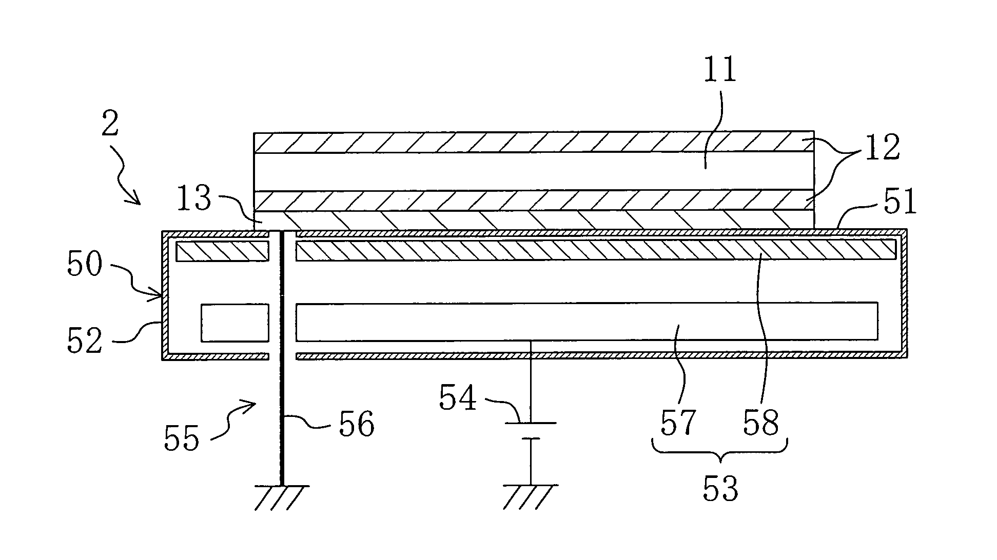
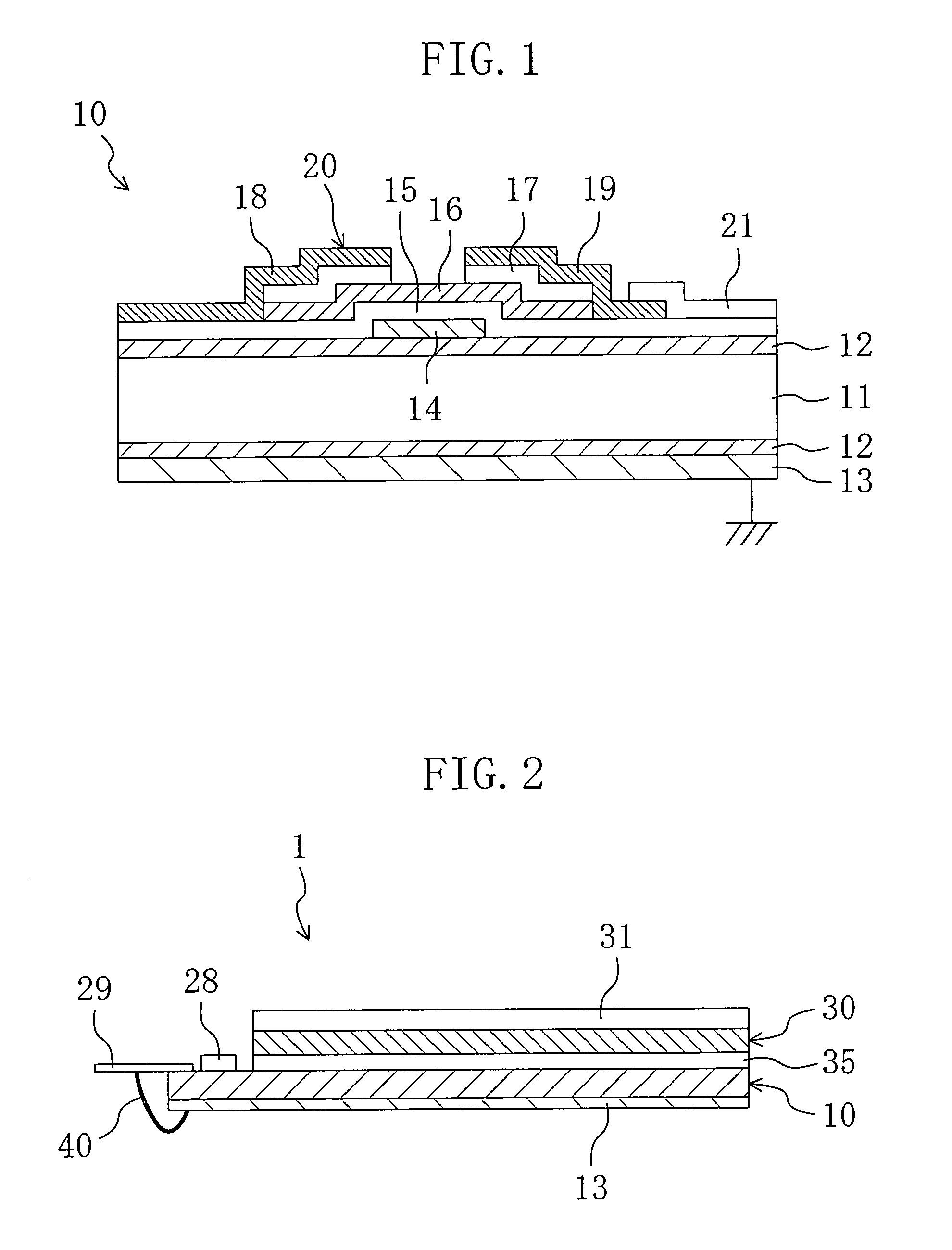
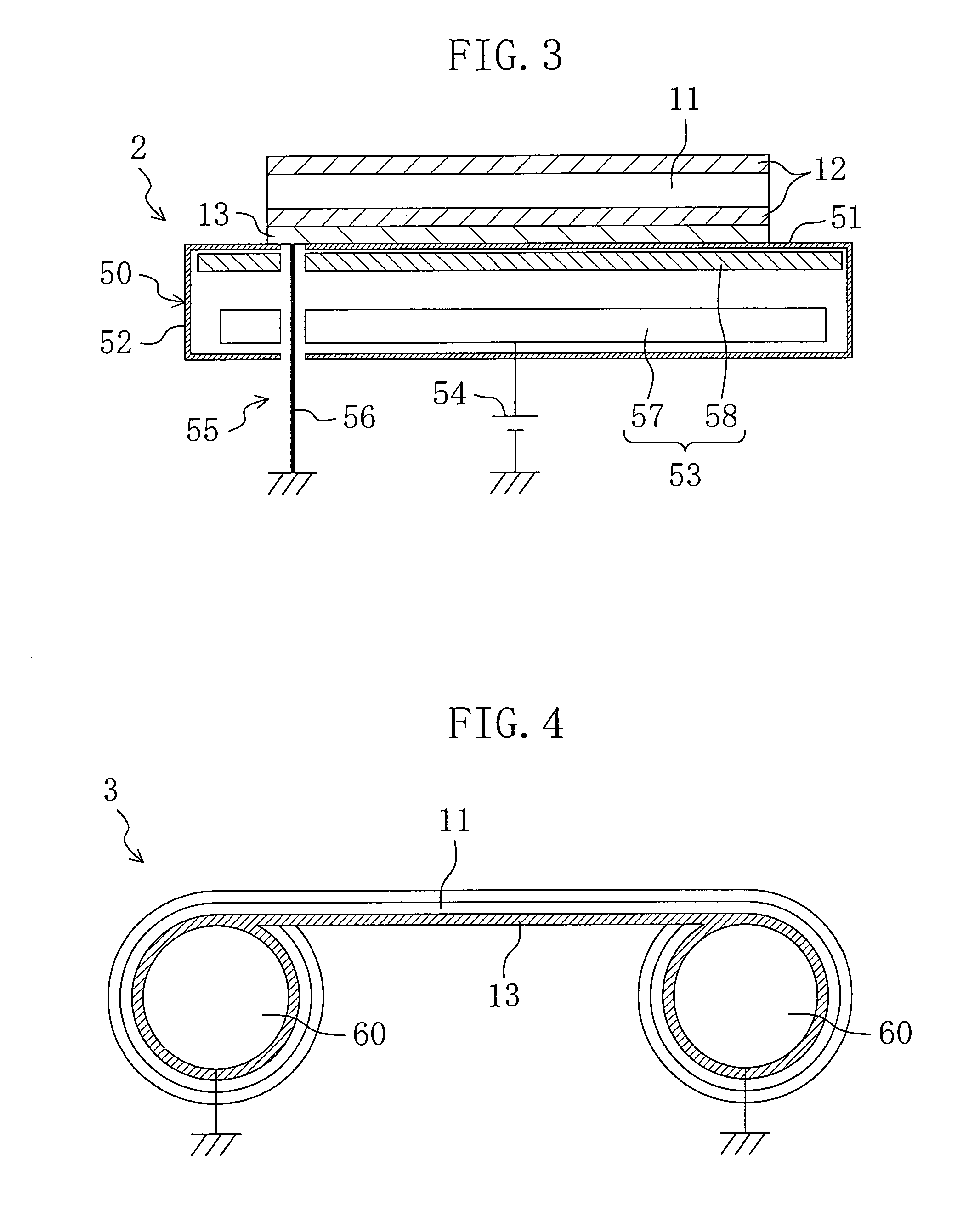
[0051]FIGS. 1 to 4 illustrate embodiments of an active matrix substrate, an apparatus for manufacturing the same and a display device using the same. FIG. 1 is an enlarged sectional view of the active matrix substrate and FIG. 2 is a schematic sectional view of the display device. Further, FIGS. 3 and 4 are sectional views illustrating major parts of the manufacturing apparatus.
[0052]First, explanation is given of the active matrix substrate and the display device including the same. The display device according to the present embodiment is a transmissive liquid crystal display 1 which is commonly used for personal computers and television sets, for example. As shown in FIG. 2, the liquid crystal display 1 includes an active matrix substrate 10 and a counter substrate 30 arranged opposite the active matrix substrate 10 with a liquid crystal layer 35 as a display medium layer interposed therebetween.
[0053]The counter substrate 30 includes a color filter (not shown). A sheet polarizer...
embodiment 2
[0095]FIG. 5 illustrates an active matrix substrate 10 according to Embodiment 2 of the present invention. In the present embodiment, the same constituents as those shown in FIGS. 1 to 4 are given with the same reference numerals and detailed explanation thereof is omitted.
[0096]Unlike Embodiment 1 in which the inorganic insulating films 12 are formed on both sides of the substrate 11, an active matrix substrate of Embodiment 2 includes only a single inorganic insulating film 12 formed on one side of the substrate 11 as shown in FIG. 5.
[0097]More specifically, the inorganic insulating film 12 is formed on the front surface of the substrate 11 in the same manner as Embodiment 1. On the other hand, the conductive film 13 is formed directly on the back surface of the substrate 11. The conductive film 13 has the function of preventing moisture permeation.
[0098]According to this configuration, the front and back sides of the substrate 11 are rendered waterproof by the inorganic insulting...
embodiment 3
[0100]FIG. 6 illustrates an active matrix substrate 10 according to Embodiment 3 of the present invention. The active matrix substrate 10 of the present embodiment is the same as that of Embodiment 1 except that a protective film 22 is added.
[0101]More specifically, the conductive film 13 is made of a conductive polymer material and the surface thereof is covered with the protective film 22. The protective film is made of an insulating film 22. The insulating film 22 may be an inorganic insulating film made of silicon nitride or silicon oxide.
[0102]The protective film 22 may be formed to cover at least part of the conductive film 13. However, for reliable protection, it is preferred that the protective film 22 covers the entire surface of the conductive film 13.
[0103]The conductive film 13 shown in FIG. 6 is not electrically grounded. However, also in this embodiment, the presence of the conductive film 13 on the substrate 11 allows dispersion of static charge over the entire surfac...
PUM
| Property | Measurement | Unit |
|---|---|---|
| thickness | aaaaa | aaaaa |
| thickness | aaaaa | aaaaa |
| temperature | aaaaa | aaaaa |
Abstract
Description
Claims
Application Information


