Microstructure, micromachine, and manufacturing method of microstructure and micromachine

a manufacturing method and micromachine technology, applied in the direction of microstructure device assembly, microstructure, transportation and packaging, etc., can solve the problems of reducing yield, buckling (also referred to as sticking) of the microstructure, and requiring an extremely long time, so as to reduce reduce the generation of various defects caused by the process of sacrificial layer etching. , the effect of reducing the time required for manufacturing

Active Publication Date: 2012-03-20
SEMICON ENERGY LAB CO LTD
View PDF23 Cites 10 Cited by
  • Summary
  • Abstract
  • Description
  • Claims
  • Application Information

AI Technical Summary

Benefits of technology

[0007]In addition, there is also a problem in that a portion, of the sacrificial layer existing below the structural layer, which has been etched, and a portion which has not been etched are generated on a substrate surface or between substrates, thereby reducing a yield. Further, there is a problem in that the variation in the size of the space portion of the microstructure formed over the substrate, that is, the distance between the substrate and the structural layer or the like is caused by the sacrificial layer etching. By steps before the sacrificial layer etching, a slight variation of a processing object over the substrate, which does not produce influence by short-time etching, is generated. The variation becomes significant by sacrificial layer etching which requires a long time, thereby greatly influencing the variation in the size of the space portion.
[0008]The thickness of the sacrificial layer is limited to a certain range. For example, when the sacrificial layer is too thick, the sacrificial layer etching takes a long time, whereas when the sacrificial layer is too thin, an etching agent does not diffuse and the sacrificial layer etching does not proceed, which causes a problem of the attachment between the structural layer and the substrate. In addition, in many cases, the area where the sacrificial layer is formed is also limited to a certain range. This is for prevention of the attachment and for reduction of time required for the sacrificial layer etching as much as possible.
[0010]Since the sacrificial layer etching adversely affects another portion, it is very hard to form the microstructure requiring the sacrificial layer etching and another component such as a semiconductor element at the same time over the same substrate. A cause of the yield of the semiconductor element and a cause of the yield of the microstructure are different. In the case of forming them over the same substrate, the yield of the completed article is the product of each yield, and the yield is reduced extremely.
[0011]The microstructure is formed from the stack of a plurality of layers, by repetition of film formation and processing of thin films having a certain thickness. In such a process, a thin film formed over a step portion generated by a lower layer has a more nonuniform film thickness compared with that of a flat portion, and a break is likely to be generated from the portion over the step portion, reducing the strength of the microstructure.
[0018]One microstructure according to the present invention is characterized in that a spacer layer and a first layer are included over a surface, the spacer layer is selectively provided between the surface and the first layer, a structural layer includes a portion fixed to the surface by the spacer layer and a portion which faces the surface with a distance therebetween. The spacer layer is provided so as to provide a noncontact portion between the first layer and the surface, making the first layer possible to move while being fixed to the surface.
[0025]In accordance with the present invention, a microstructure can be formed without sacrificial layer etching. In other words, since a similar step to the sacrificial layer etching is conducted in the separation and the attachment, the step can be completed in a considerably short time. In addition, the microstructure does not contact a liquid etchant as in wet etching, and accordingly a microstructure can be formed so as not to generate attachment of a structural layer and a substrate by a capillary phenomenon. When applying the present invention in this way, the time required for the manufacture can be reduced and generation of various defects caused by the process called sacrificial layer etching can be reduced.

Problems solved by technology

As well as being an important step in manufacturing a microstructure, the sacrificial layer etching is a rate-controlling point with many problems.
First, the most common problem in the sacrificial layer etching is that it requires an extremely long time.
Further, another reason is that the sacrificial layer etching is conducted using isotropic etching, since the sacrificial layer has a complicate shape of existing below the structural layer.
However, the sacrificial layer etching using a liquid has a problem in that at the time of drying after the sacrificial layer etching, a structural layer and a substrate attach to each other by a capillary phenomenon and buckling (also referred to as sticking) of the microstructure is caused.
In addition, there is also a problem in that a portion, of the sacrificial layer existing below the structural layer, which has been etched, and a portion which has not been etched are generated on a substrate surface or between substrates, thereby reducing a yield.
Further, there is a problem in that the variation in the size of the space portion of the microstructure formed over the substrate, that is, the distance between the substrate and the structural layer or the like is caused by the sacrificial layer etching.
The variation becomes significant by sacrificial layer etching which requires a long time, thereby greatly influencing the variation in the size of the space portion.

Method used


Image

  • Microstructure, micromachine, and manufacturing method of microstructure and micromachine
  • Microstructure, micromachine, and manufacturing method of microstructure and micromachine
  • Microstructure, micromachine, and manufacturing method of microstructure and micromachine

Examples


embodiment mode 1

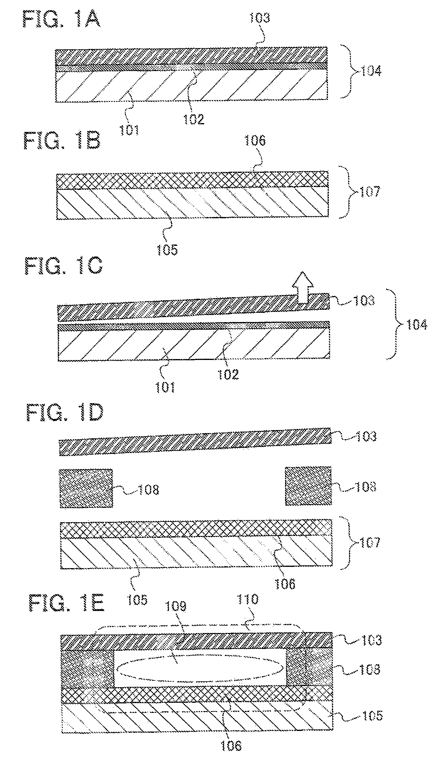
[0066]In Embodiment Mode 1, a manufacturing method of a microstructure of the present invention will be described.

[0067]First, with reference to FIGS. 1A to 1E, a manufacturing method of a microstructure of the present invention and a separation method which is important in carrying out the manufacturing method will be described. Here, the drawings are substrate cross sectional views.

[0068]In order to manufacture the microstructure of the present invention, a separation layer 102 and a first layer 103 are formed over a first substrate (also referred to as a first support substrate) 101 first, as shown in FIG. 1A so that a substrate including the first layer 104 is manufactured. Then, as shown in FIG. 1B, a second layer 106 is formed over a second substrate (also referred to as a first protective substrate) 105 to manufacture a substrate including the second layer 107.

[0069]Then, as shown in FIG. 1C, the first layer 103 is separated from the substrate including the first layer 104, u...

embodiment mode 2

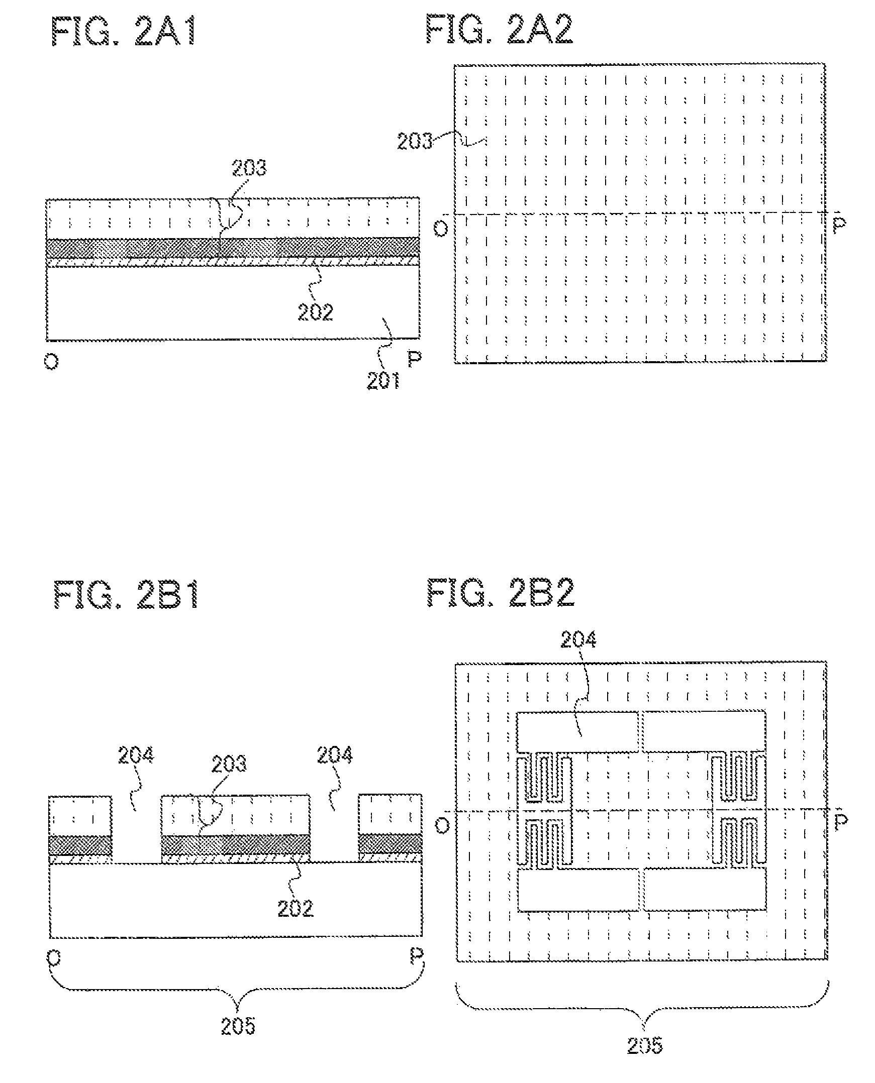
[0086]Embodiment Mode 2 will concretely describe a manufacturing method of the microstructure described in Embodiment Mode 1, with reference to FIGS. 2A1 to 4C2. Note that the drawings on the right side are top views of substrates and the drawings on the left side are cross sectional views taken along a dashed line O-P of the top views.

[0087]First, a processing method of one substrate having a first layer will be described with reference to FIGS. 2A1 and 2B2.

[0088]As shown in FIGS. 2A1 and 2A2, a separation layer 202 is formed over a first substrate (also referred to as a first support substrate) 201. Here, various substrates such as a substrate having an insulating property, for example, of glass, quartz, or plastic, or a substrate having a conductive property such as metal, as well as a substrate having a semiconductor property such as a silicon substrate can be used for the first substrate 201.

[0089]The separation layer 202 is formed by a CVD method, a sputtering method, or the l...

embodiment mode 3

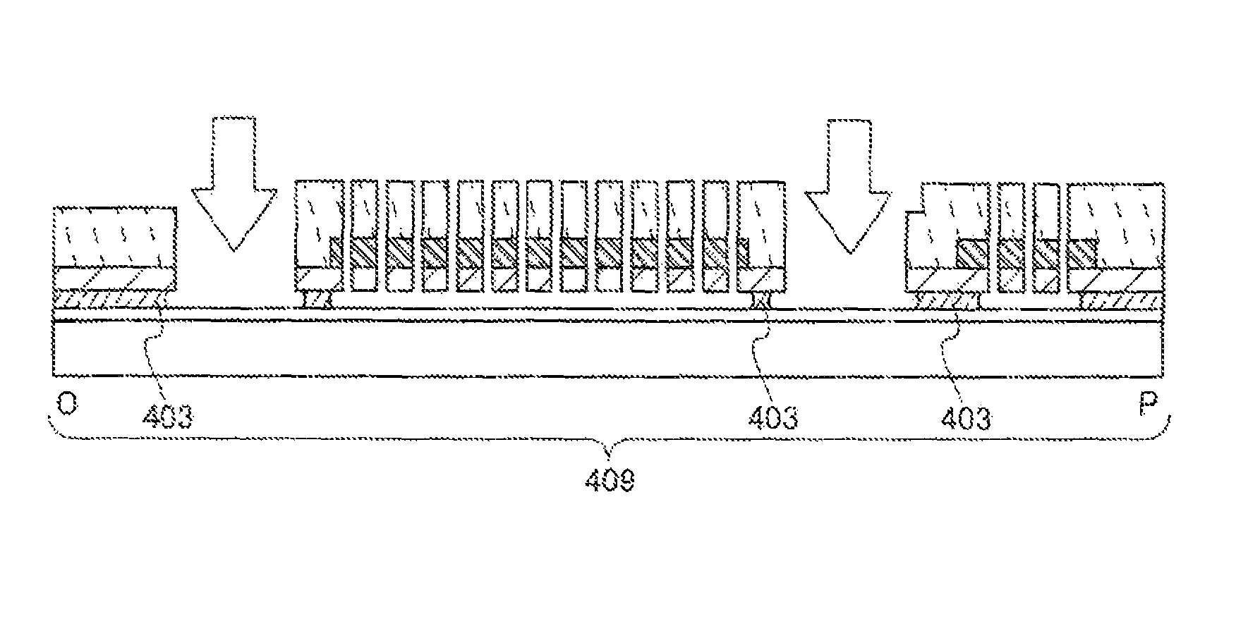
[0118]In Embodiment Mode 3, an example for manufacturing a microstructure, which employs the method described in Embodiment Mode 1, will be described with reference to FIGS. 5A to 9C. Here, the drawings are cross sectional views.

[0119]As shown in FIG. 5A, a first separation layer 302 and a first layer 303 are formed over a first substrate (also referred to as a first support substrate) 301 to form a substrate including the first layer 304. As shown in FIG. 5B, the first layer 303 is separated from the substrate including the first layer 304 at an interface of the first separation layer 302.

[0120]Next, a first spacer layer 306 is selectively formed over a second substrate 305, and a second spacer layer 308 is selectively formed over a third substrate 307. The second substrate 305 including the first spacer layer 306 and the third substrate 307 including the second spacer layer 308 are attached to each other so as to interpose the first layer 303 therebetween (FIG. 5C).

[0121]Thus, the...


PUM

PropertyMeasurementUnit
thicknessaaaaaaaaaa
thicknessaaaaaaaaaa
thicknessaaaaaaaaaa

Abstract

Without sacrificial layer etching, a microstructure and a micromachine are manufactured. A separation layer 102 is formed over a substrate 101, and a layer 103 to be a movable electrode is formed over the separation layer 102. At an interface of the separation layer 102, the layer 103 to be a movable electrode is separated from the substrate. A layer 106 to be a fixed electrode is formed over another substrate 105. The layer 103 to be a movable electrode is fixed to the substrate 105 with the spacer layer 103 which is partially provided interposed therebetween, so that the layer 103 to be a movable electrode and a layer 106 to be a fixed electrode face each other.

Description

TECHNICAL FIELD[0001]The present invention relates to a microstructure for forming a micromachine, a micromachine, and a semiconductor device. Further, the present invention relates to a manufacturing method of a microstructure and a micromachine including a microstructure.BACKGROUND ART[0002]A micromachine is also called MEMS (Micro Electro Mechanical System) or MST (Micro System Technology) and refers to a comprehensive system combining a minute mechanical microstructure and an electric circuit. The above-described microstructure is different from a general semiconductor element and has a three-dimensional structure, and a part of the microstructure is movable in many cases. The micromachine can have various functions of a passive element such as a sensor, an actuator, an inductor, or a variable capacitor, a switch, or the like. The electric circuit is generally formed using a semiconductor element and can control the operation of the microstructure, or receive and process a weak ...

Claims


Application Information

Patent Timeline
Patent Type & Authority Patents(United States)
IPC IPC(8): H01L21/00
CPCB81C3/008H01L21/762B32B38/10B81C2201/019Y10T428/24802
Inventor YAMAGUCHI, MAYUMIIZUMI, KONAMI
Owner SEMICON ENERGY LAB CO LTD
Why Eureka
Try Eureka