
Semiconductor memory device for self refresh and memory system having the same

a memory device and memory technology, applied in the field of semiconductor memory devices, can solve problems such as data loss, storage contents are lost, stored data is not maintained,

Active Publication Date: 2012-03-27
SAMSUNG ELECTRONICS CO LTD
View PDF5 Cites 5 Cited by
  • Summary
  • Abstract
  • Description
  • Claims
  • Application Information

AI Technical Summary

Benefits of technology

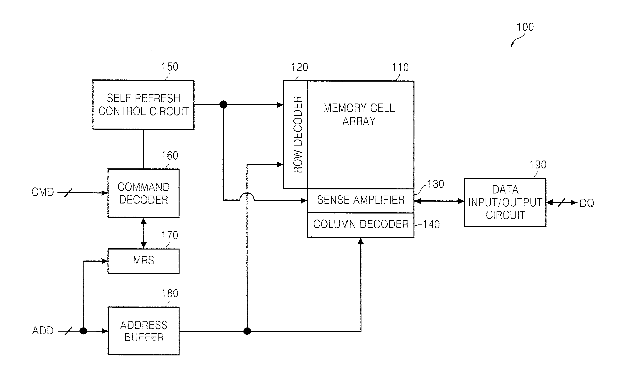
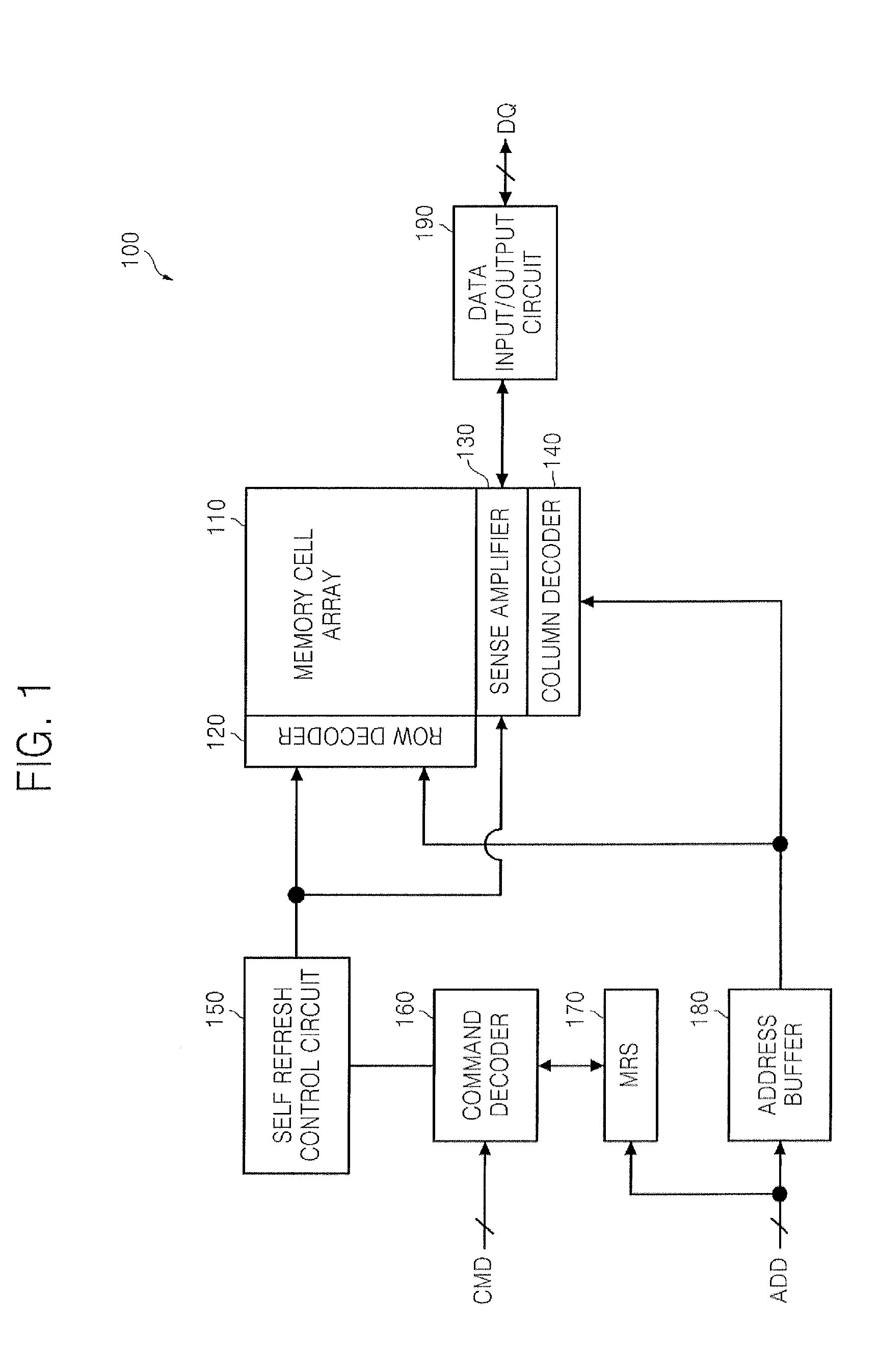
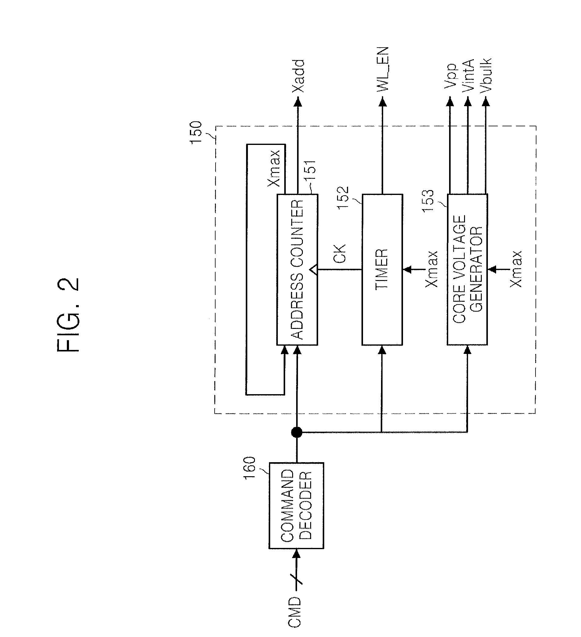
The present invention provides a semiconductor memory device that can firmly restore data of a weak cell by self refresh operation. The device includes a memory core unit with a memory cell array and a sense amplifier to sense and amplify data of the memory cells. A self refresh control unit applies at least one first core voltage to the memory core unit and controls a self refresh operation to be performed at every first self refresh cycle, and applies at least one second core voltage to the memory core unit and controls the self refresh operation to be performed at every second self refresh cycle. The self refresh control unit includes a timer, an address counter, and a core voltage generator to generate the core voltage of a first level based on a self refresh entry command. The device also includes a controller to generate a control signal to control the self refresh control unit to perform the refresh operation. The technical effect of the invention is to improve the reliability and performance of the semiconductor memory device by ensuring the data of weak cells is restored effectively.

Problems solved by technology

The volatile semiconductor memory device exhibits fast read and write speeds but the stored contents are lost when an external power supply is discontinued.
That is, for a memory cell for storing data in the volatile semiconductor memory device, the stored data is not maintained over a predetermined time because of its intrinsic leakage current.
Thus, when the refresh cycle is slow, data may be lost.
When the refresh cycle is excessively fast, the consumption of power increases.
When, during a data write operation, a sufficient amount of charges is not stored in the memory cell due to insufficient data write time or insufficient voltage, the memory cell may become a weak cell that is highly likely to lose data.
When the weak cell exists and further the refresh cycle is slow, data loss possibility may increase accordingly.

Method used


Image

  • Semiconductor memory device for self refresh and memory system having the same
  • Semiconductor memory device for self refresh and memory system having the same
  • Semiconductor memory device for self refresh and memory system having the same

Examples


Embodiment Construction

[0032]The attached drawings for illustrating embodiments of the inventive concept are referred to in order to gain a sufficient understanding of the inventive concept and the merits thereof. Hereinafter, the inventive concept will be described in detail by explaining embodiments of the inventive concept with reference to the attached drawings. Like reference numerals in the drawings denote like elements.

[0033]Reference will now be made in detail to the embodiments of the present general inventive concept, examples of which are illustrated in the accompanying drawings, wherein like reference numerals refer to the like elements throughout. The embodiments are described below in order to explain the present general inventive concept by referring to the figures.

[0034]It will be understood that when an element is referred to as being “connected” or “coupled” to another element, it can be directly connected or coupled to the other element or intervening elements may be present. In contras...


PUM


Abstract

A semiconductor memory device includes a memory core unit including a memory cell array including a plurality of memory cells and a sense amplifier to sense and amplify data of the plurality of memory cells, and a self refresh control unit to apply at least one first core voltage to the memory core unit and to control a self refresh operation to be performed at every first self refresh cycle, in a first self refresh mode, and to apply at least one second core voltage to the memory core unit and to control the self refresh operation to be performed at every second self refresh cycle, in a second self refresh mode. In the semiconductor memory, a level of the at least one first core voltage is higher than that of a corresponding one of the at least one second core voltage, and the first self refresh cycle is shorter than the second self refresh cycle.

Description

CROSS-REFERENCE TO RELATED APPLICATIONS[0001]This application claims priority under 35 U.S.C. §119 of Korean Patent Application No. 10-2008-0134019, filed on 26 Dec. 2008, in the Korean Intellectual Property Office, the disclosure of which is incorporated herein in its entirety by reference.BACKGROUND[0002]1. Field of the Invention[0003]The inventive concept relates to a semiconductor memory device, and more particularly, to a device to improve data restoration capability in a volatile semiconductor device such as a dynamic random access memory (DRAM).[0004]2. Description of the Related Art[0005]Semiconductor memory devices include volatile semiconductor memory devices and non-volatile semiconductor memory devices. The volatile semiconductor memory device exhibits fast read and write speeds but the stored contents are lost when an external power supply is discontinued. That is, for a memory cell for storing data in the volatile semiconductor memory device, the stored data is not mai...

Claims


Application Information

Patent Timeline
Patent Type & Authority Patents(United States)
IPC IPC(8): G11C7/00
CPCG11C11/406G11C11/40615G11C11/401G11C11/402G11C11/4074
Inventor LIM, JONG HYOUNGKANG, SANG SEOK
Owner SAMSUNG ELECTRONICS CO LTD
Learn More