Light absorption layer for a display device

a technology of light absorption layer and display device, which is applied in the direction of thin material processing, instruments, chemistry apparatus and processes, etc., to achieve the effect of preventing alignment spots

Active Publication Date: 2012-04-03
SAMSUNG DISPLAY CO LTD
View PDF2 Cites 3 Cited by
  • Summary
  • Abstract
  • Description
  • Claims
  • Application Information

AI Technical Summary

Benefits of technology

[0012]Accordingly, the present invention increases the alignment stability by forming the overcoat on the upper substrate.
[0040]Accordingly, in the liquid crystal display according to an exemplary embodiment of the present invention, the overcoat absorbs light of the wavelength of the specific region generated from external lights such that it is prevented that the pre-tilt of the light alignment layer is changed, thereby preventing alignment spots.

Problems solved by technology

A disadvantage of this method is that minute particles or an electrostatic discharge (ESD) may be generated when the fiber and the polymer layer are rubbed against each other, and they may cause a serious problem during the manufacturing of the liquid crystal panel.

Method used


Image

  • Light absorption layer for a display device
  • Light absorption layer for a display device
  • Light absorption layer for a display device

Examples


Embodiment Construction

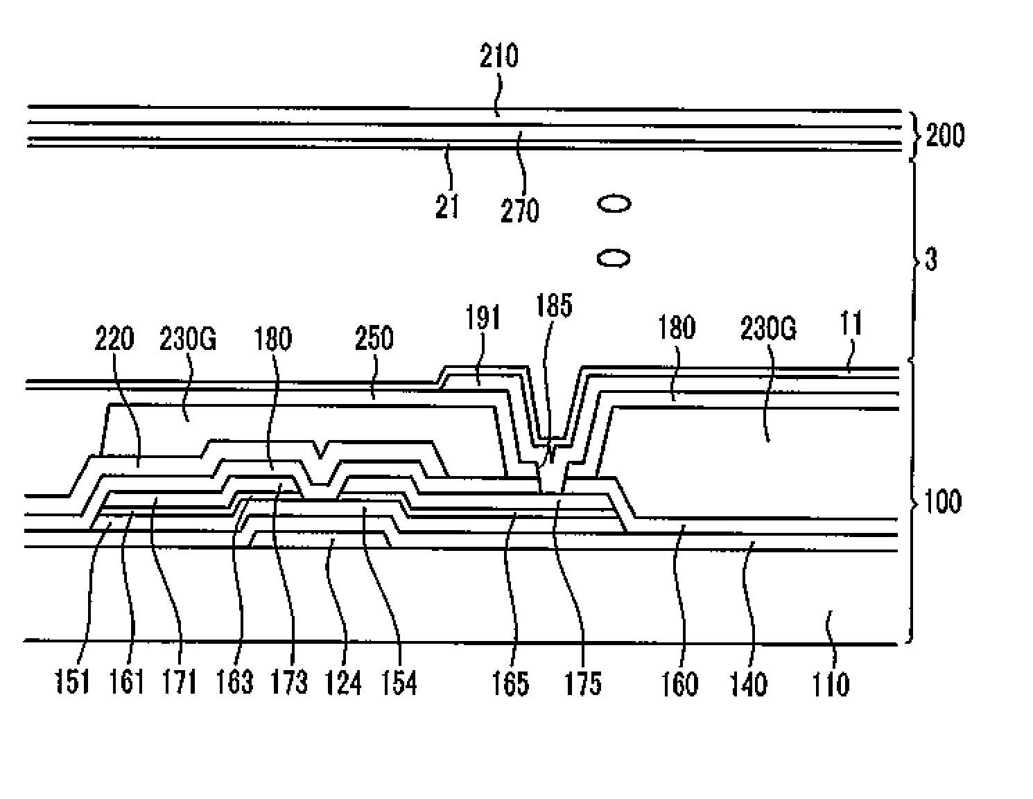
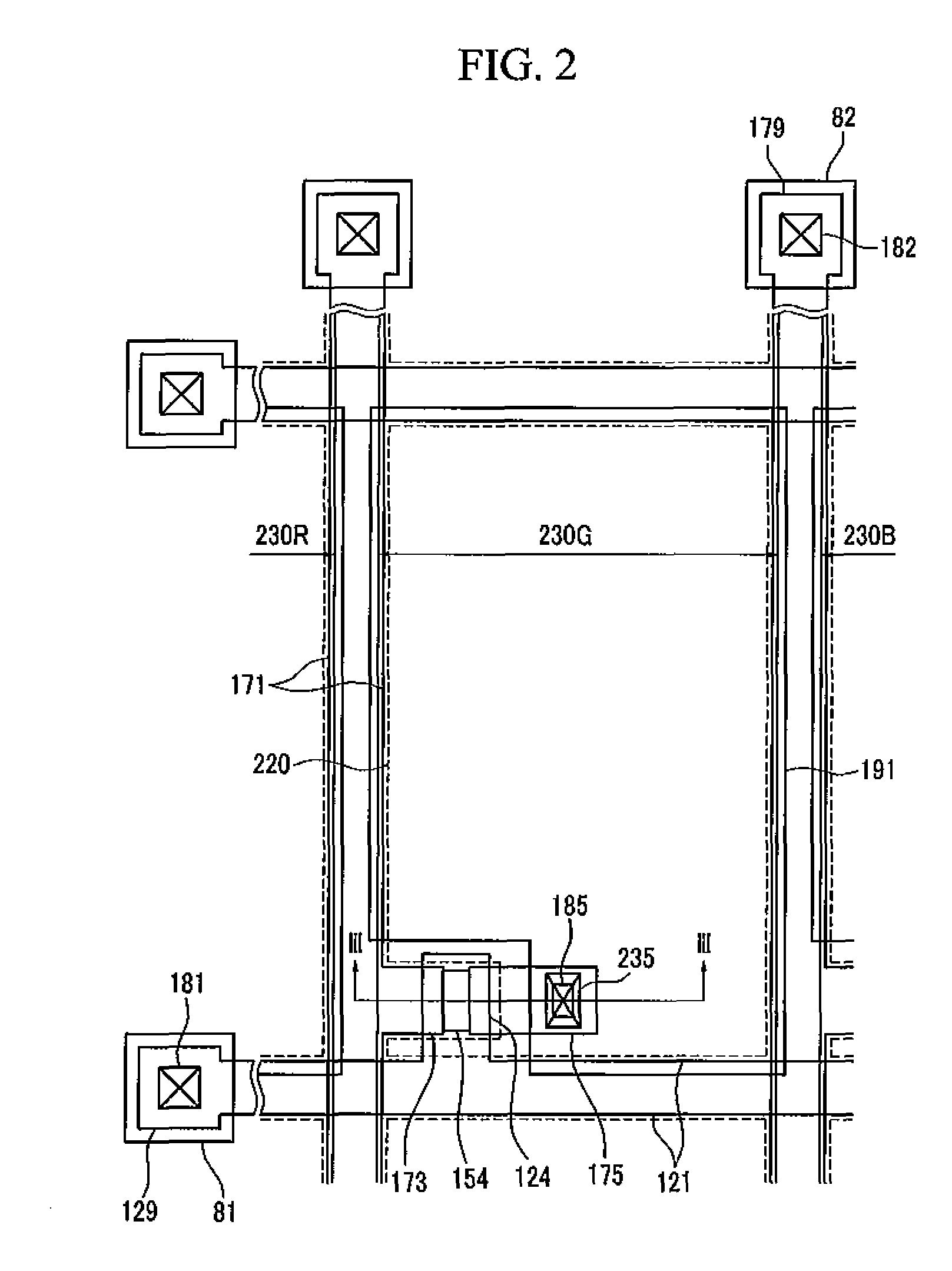
[0048]An exemplary embodiment of the present invention will hereinafter be described in detail with reference to the accompanying drawings. As those skilled in the art would realize, the described embodiments may be modified in various different ways, all without departing from the spirit or scope of the present invention. The present exemplary embodiments provide complete disclosure of the present invention and complete information of the scope of the present invention to those skilled in the art.

[0049]In the drawings, the thickness of layers, films, panels, regions, etc., are exaggerated for clarity. Like reference numerals designate like elements throughout the specification. It will be understood that when an element such as a layer, film, region, or substrate is referred to as being “on” another element, it can be directly on the other element or intervening elements may also be present.

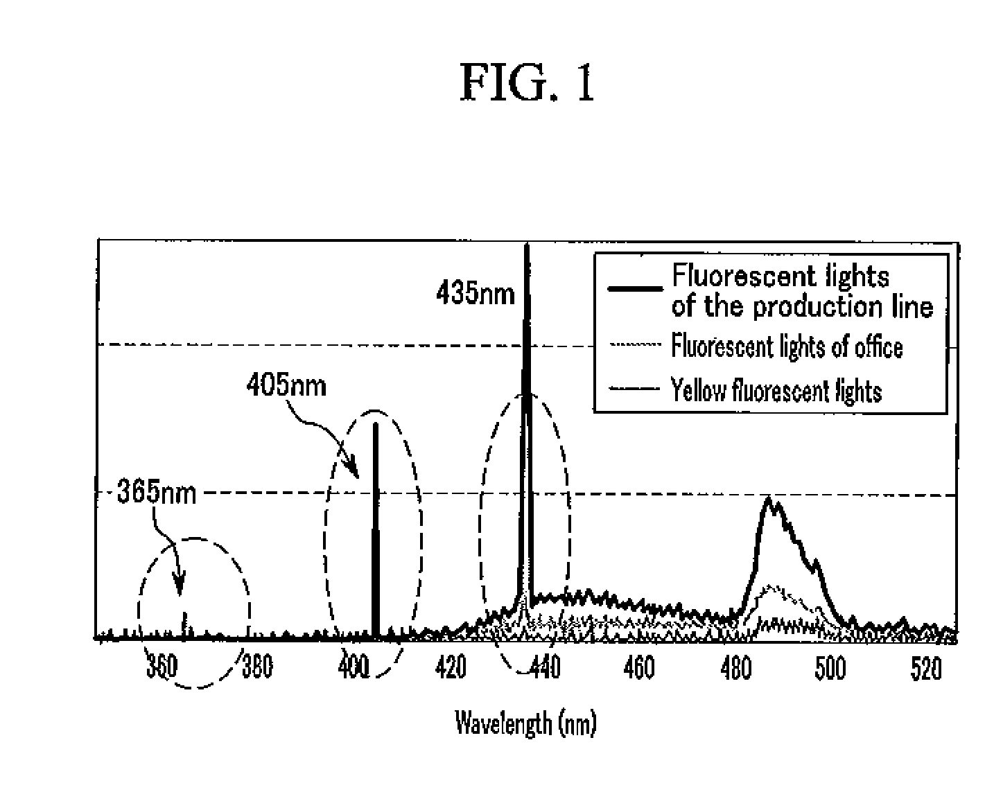
[0050]FIG. 1 is a graph showing a wavelength spectrum generated according to the kind of ext...


PUM

PropertyMeasurementUnit
UV wavelengthaaaaaaaaaa
wavelengthaaaaaaaaaa

Abstract

A liquid crystal display is presented. The liquid crystal display includes: a first substrate; a pixel electrode formed on the first substrate; a first alignment layer formed on the pixel electrode; a second substrate facing the first substrate; a common electrode formed on the second substrate; a second alignment layer formed on the common electrode; a liquid crystal layer formed between the first alignment layer and the second alignment layer; and a light absorption layer formed between the first substrate and the first alignment layer, or the second substrate and the second alignment layer, wherein the light absorption layer absorbs light having a UV wavelength between about 280 nm and about 450 nm.

Description

CROSS-REFERENCE TO RELATED APPLICATION[0001]This application claims priority to and the benefit of Korean Patent Application No. 10-2008-0076450 filed in the Korean Intellectual Property Office on Aug. 5, 2008, the entire content of which is incorporated herein by reference.BACKGROUND OF THE INVENTION[0002](a) Field of the Invention[0003]The present invention relates to a liquid crystal display including an overcoat layer.[0004](b) Description of the Related Art[0005]In a liquid crystal element, images are displayed by switching the orientation of liquid crystals between transparent conductive glass surfaces through an external electric field. The liquid crystals are aligned in a predetermined direction at the interface between the liquid crystals and the transparent conductive glass surface. The degree of uniformity in the liquid crystal alignment is an important factor for determining the display quality of the liquid crystal display.[0006]Rubbing is a conventional method of align...

Claims


Application Information

Patent Timeline
Patent Type & Authority Patents(United States)
IPC IPC(8): G02F1/1335
CPCG02F1/13378Y10T428/1036G02F2201/086G02F1/133788C09K2323/03G02F1/1337G02F1/1343
Inventor CHOI, NAK-CHOKANG, MINKANG, HOON
Owner SAMSUNG DISPLAY CO LTD
Why Eureka
Try Eureka