Fabrication of semiconductor structure having asymmetric field-effect transistor with tailored pocket portion along source/drain zone

a field-effect transistor and pocket portion technology, applied in the field of field-effect transistors, can solve the problems of weakened analog performance, difficult to incorporate choi's process into a larger semiconductor process, and the inability to control the operation of the igfet with its gate electrode, etc., and achieve the effect of reducing leakage current and being easily integrated into a semiconductor fabrication platform

Active Publication Date: 2012-04-24
NAT SEMICON CORP
View PDF17 Cites 118 Cited by
  • Summary
  • Abstract
  • Description
  • Claims
  • Application Information

AI Technical Summary

Benefits of technology

[0039]The present invention furnishes a semiconductor structure that contains an asymmetric IGFET having a halo pocket portion specially tailored to reduce off-state source / drain leakage current. The present asymmetric IGFET is especially suitable for applications, typically analog applications, in which the channel-zone current flow is always in the same direction. Tailoring the halo pocket to reduce off-state source / drain leakage current normally does not significantly affect any other part of the IGFET's fabrication. As a result, the asymmetric IGFET of the invention can readily be incorporated into a semiconductor fabrication platform that provides high-performance digital IGFETs as well as IGFETs with good analog characteristics.
[0042]Doping the pocket portion in the preceding way according to the invention's teachings enables the vertical dopant profile in the pocket portion to be flatter near the upper semiconductor surface than occurs in similarly configured prior art asymmetric IGFETs in which the pocket portion reaches a maximum concentration along only a single location. The concentration of the dopant of the first conductivity type in the IGFET of the invention preferably varies by a factor of no more than 2.5 in moving largely from the upper semiconductor surface to the location of the deepest local maxima in the concentration of the dopant of the first conductivity type along the imaginary vertical line. Due to this flattening of the pocket portion's vertical dopant profile near the upper semiconductor surface, less leakage current flows between the IGFET's S / D zones when the IGFET is in its biased-off state.
[0043]Each S / D zone normally contains a main portion and a more lightly doped lateral extension laterally continuous with the main S / D portion. Each S / D extension extends laterally under the gate electrode such that the channel zone is terminated by the S / D extensions along the body's upper surface. Usage of lateral S / D extensions, especially for the S / D zone acting as the IGFET's drain, generally reduces hot carrier injection into the IGFET's gate dielectric layer. Undesired threshold-voltage drift with operational time is thereby reduced. The IGFET operates very efficiently.
[0044]The S / D extensions of the first and second S / D zones are preferably respectively largely defined by first and second semiconductor dopants of the second conductivity type. The first dopant of the second conductivity type is of higher atomic weight than the second dopant of the second conductivity type. With the first S / D zone acting as the source, the higher atomic weight of the first dopant of the second conductivity type leads to a reduction in the source resistance of the IGFET so that its transconductance is advantageously increased. The lower atomic weight of the second dopant of the second conductivity type leads to a reduction in the peak value of the electric field in the S / D extension of the second S / D zone. With the second S / D zone acting as the drain, the IGFET has better high-voltage reliability.
[0050]In short, off-state leakage current is significantly reduced in the present IGFET by tailoring the vertical dopant profile in the pocket portion to be relatively flat near the upper semiconductor surface. Due to its asymmetric nature, the IGFET of the invention is particularly suitable for analog applications. The present IGFET is preferably fabricated in such a manner that it can readily be incorporated into a semiconductor fabrication platform which provides high-performance digital and analog IGFETs. The invention thus provides a significant advance over the prior art.

Problems solved by technology

When surface or bulk punchthrough occurs, the operation of the IGFET cannot be controlled with its gate electrode.
However, Choi's coupling of the formation of gate electrode 46 with the formation of source / drain extensions 26E and 28E in the process of FIG. 10 is laborious and could make it difficult to incorporate Choi's process into a larger semiconductor process that provides other types of IGFETs.
Although it would be economically attractive to utilize the same transistors for the analog and digital blocks, doing so would typically lead to weakened analog performance.
Many requirements imposed on analog IGFET performance conflict with the results of digital scaling.
Hence, linearity demands on analog transistors are very high.
Because the resultant dimensional spreads are inherently large, parameter matching in digital circuitry is often relatively poor.

Method used


Image

  • Fabrication of semiconductor structure having asymmetric field-effect transistor with tailored pocket portion along source/drain zone
  • Fabrication of semiconductor structure having asymmetric field-effect transistor with tailored pocket portion along source/drain zone
  • Fabrication of semiconductor structure having asymmetric field-effect transistor with tailored pocket portion along source/drain zone

Examples


Embodiment Construction

List of Contents

[0102]A. Reference Notation and Other Preliminary Information

[0103]B. Complementary-IGFET Structures Suitable for Mixed-signal Applications

[0104]C. Well Architecture and Doping Characteristics

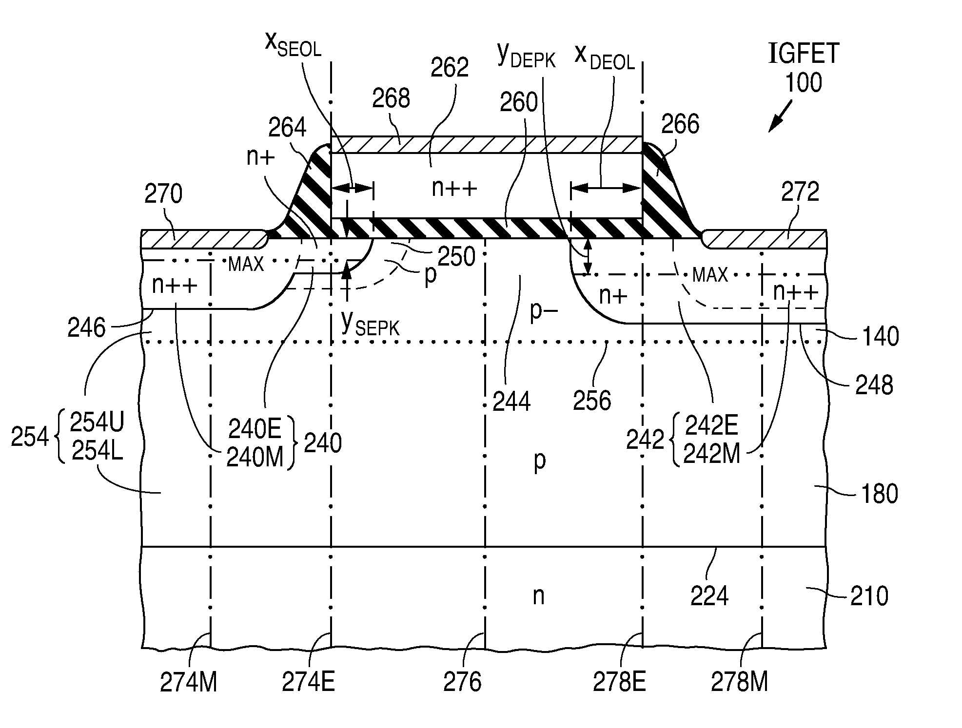
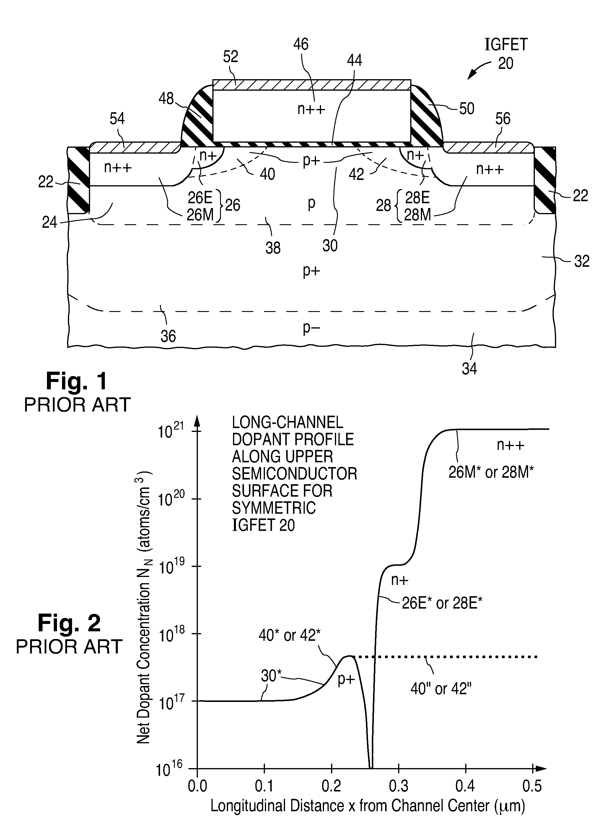
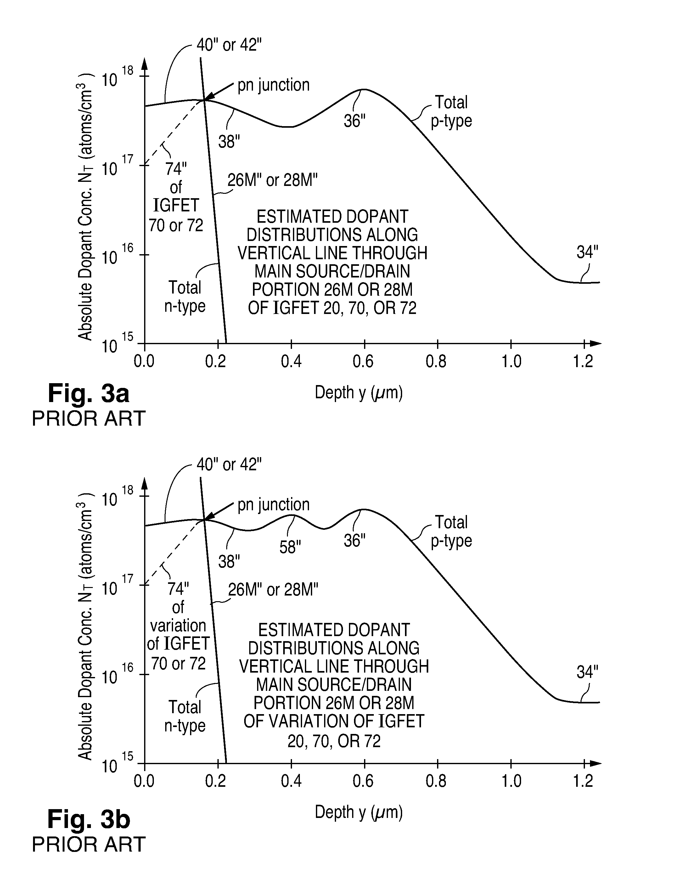
[0105]D. Asymmetric High-voltage IGFETs[0106]D1. Structure of Asymmetric High-voltage N-channel IGFET[0107]D2. Source / Drain Extensions of Asymmetric High-voltage N-channel IGFET[0108]D3. Different Dopants in Source / Drain Extensions of Asymmetric High-voltage N-channel IGFET[0109]D4. Dopant Distributions in Asymmetric High-voltage N-channel IGFET[0110]D5. Structure of Asymmetric High-voltage P-channel IGFET[0111]D6. Source / Drain Extensions of Asymmetric High-voltage P-channel IGFET[0112]D7. Different Dopants in Source / Drain Extensions of Asymmetric High-voltage P-channel IGFET[0113]D8. Dopant Distributions in Asymmetric High-voltage P-channel IGFET[0114]D9. Common Properties of Asymmetric High-voltage IGFETs[0115]D10. Performance Advantages of Asymmetric High-voltage IGFETs[0116]...


PUM


Abstract

An asymmetric insulated-gate field effect transistor (100U or 102U) is provided along an upper surface of a semiconductor body so as to have first and second source / drain zones (240 and 242 or 280 and 282) laterally separated by a channel zone (244 or 284) of the transistor's body material. A gate electrode (262 or 302) overlies a gate dielectric layer (260 or 300) above the channel zone. A pocket portion (250 or 290) of the body material more heavily doped than laterally adjacent material of the body material extends along largely only the first of the S / D zones and into the channel zone. The vertical dopant profile of the pocket portion is tailored to reach a plurality of local maxima at respective locations (PH-1-PH-3-NH-3) spaced apart from one another. This typically enables the transistor to have reduced current leakage.

Description

CROSS-REFERENCE TO RELATED APPLICATIONS[0001]This application is related to the following U.S. patent applications all filed on the same date as this application: U.S. patent application Ser. No. 12 / 382,973 (Bulucea et al.), U.S. patent application Ser. No. 12 / 382,976 (Bahl et al.), U.S. patent application Ser. No. 12 / 382,977 (Parker et al.), now allowed, U.S. patent application Ser. No. 12 / 382,972 (Bahl et al.), now U.S. Pat. No. 7,973,372 B2, U.S. patent application Ser. No. 12 / 382,966 (Yang et al.), now U.S. Pat. No. 8,030,151 B2, U.S. patent application Ser. No. 12 / 382,968 (Bulucea et al.), U.S. patent application Ser. No. 12 / 382,969 (Bulucea et al.) , now U.S. Pat. No. 7,968,921 B2, U.S. patent application Ser. No. 12 / 382,974 (French et al.), U.S. patent application Ser. No. 12 / 382,971 (Bulucea et al.), now U.S. Pat. No. 8,084,827, and U.S. patent application Ser. No. 12 / 382,970 (Chaparala et al.). To the extent not repeated herein, the contents of these other applications are ...

Claims


Application Information

Patent Timeline
Patent Type & Authority Patents(United States)
IPC IPC(8): H01L21/336
CPCH01L21/26513H01L21/2652H01L21/823807H01L21/823814H01L21/823892H01L27/0922H01L29/0847H01L29/1045H01L29/1083H01L29/66659H01L29/7835H01L21/26586H01L29/0653H01L29/105H01L29/665H01L21/2658
Inventor YANG, JENG-JIUNBULUCEA, CONSTANTINBAHL, SANDEEP R.
Owner NAT SEMICON CORP
Why Eureka
Try Eureka