Method for fabricating 3D microstructure

a 3d microstructure and microstructure technology, applied in the field of 3d microstructure fabrication, can solve the problems of low precision, unsuitable for fabricating novel optics, and low precision, and achieve the effects of reducing process equipment costs, facilitating large-area fabrication of 3d microstructures, and reducing diffraction errors

Active Publication Date: 2012-05-01
NAT SYNCHROTRON RADIATION RES CENT
View PDF1 Cites 10 Cited by
  • Summary
  • Abstract
  • Description
  • Claims
  • Application Information

AI Technical Summary

Benefits of technology

[0012]In order to resolve the foregoing problems, one object of this invention is to provide a method for fabricating 3D microstructure, wherein a matching fluid is arranged between the mask and the photoresist layer. When the mask and photoresist layer proceed the relative scanning and the exposure process simultaneously, the matching fluid will reduce the diffraction error, so that the gap between the mask and the photoresist layer becomes more tolerable. The matching fluid also acts as a lubricant for achieving a smooth scanning motion. All these features will substantially relax the requirements for the stage precision and the resist's thickness uniformity, reduce the expense for the process equipment, and facilitate large-area fabrication of 3D microstructure.
[0013]One object of this invention is to provide a method for fabricating 3D microstructure, wherein because of the use of the matching fluid, a simple UV light may be used as an exposure source without using any expensive light source, to have the advantage of the low cost.
[0014]One object of this invention is to provide a method for fabricating 3D microstructure. Compared to the direct-writing lithography which uses a laser, e-beam or ion beam and takes a long time to fabricate 3D microstructure, the present invention may fabricate a high-precision and a large-area 3D optical microstructure in a comparatively short time.

Problems solved by technology

However, this technique can only applied for fabricating 3D microstructure with simple geometry and low precision; It is then not suitable to fabricate novel optics, such as a hybrid lens combining refractive / diffractive functions.
This is a simple method, but it is very time-consuming and is not ideal for obtaining reproducible quality.
In this technique, the lithographic process is rather simple, however complex optical simulation, compensation and fabrication processes are required for fabricating the grey-tone mask, in which is very expensive.
If the gap is too large, the diffraction error is increased to affect the fabrication precision.
If the gap is too small, the friction between the mask and the photoresist would destroy the resist surface and hamper the scanning motion.
Synchrotron X-ray was traditionally used as a light source due to its small diffraction error, but the synchrotron source is limited and the vacuum chamber for exposure is not easy to be scaled-up and therefore is unfavorable for fabricating large-area optical device.
However, when the gap is substantially reduced (<50 μm), the thickness uniformity of the photoresist layer and the machine precision are critical, which would markedly increase the cost of scanning stage and therefore unfavorable for fabricating large-area 3D microstructure.
It is observed that the cross-section of the microstructure 10 is rather irregular and the surface quality is poor, which is not adequate for fabricating high-precision 3D microstructures.

Method used


Image

  • Method for fabricating 3D microstructure
  • Method for fabricating 3D microstructure
  • Method for fabricating 3D microstructure

Examples


Embodiment Construction

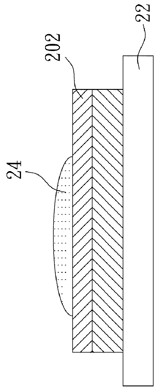
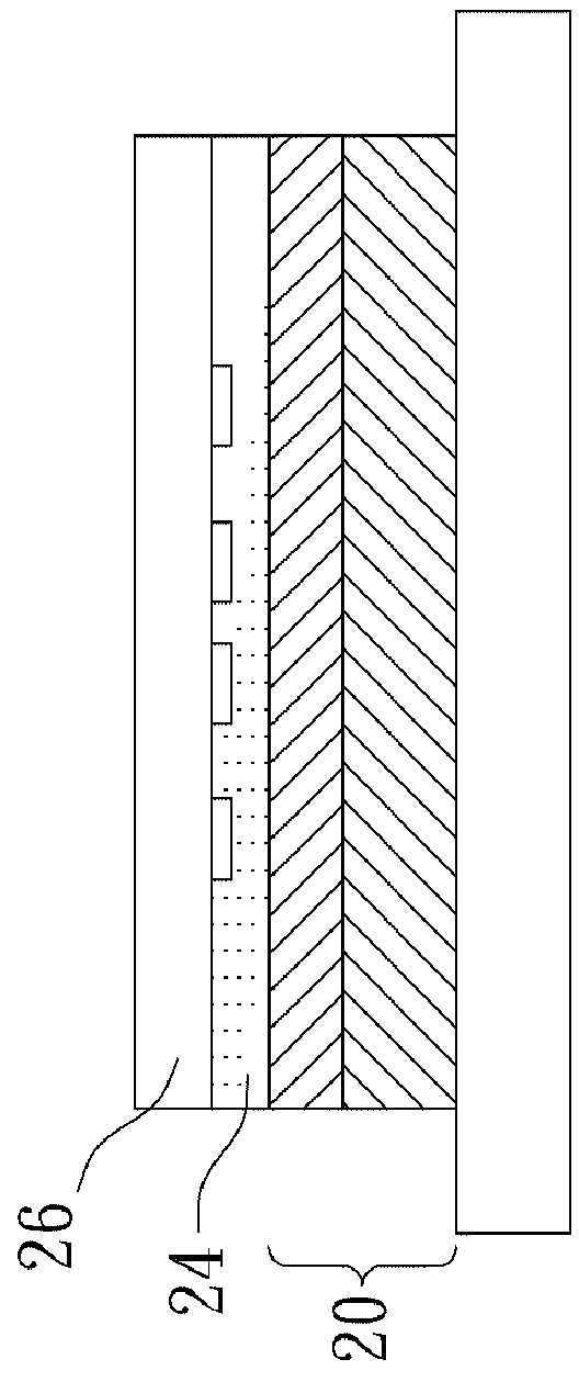
[0020]FIG. 2a to FIG. 2e illustrates a flow of a method for fabricating a 3D microstructure in accordance with an example embodiment of the present invention. First, as illustrated in FIG. 2a, a photoresist strip 20 is provided. In one example embodiment, the photoresist strip 20 is configured on a moving stage 22. The photoresist strip 20 includes a substrate 201 and a photoresist layer 202 which is uniformly arranged on the substrate 201 by spin coating and soft bake process, wherein the material of the photoresist layer 202 may be a positive photosensitive material or a negative photosensitive material, and the thickness of the photoresist layer 202 is determined according to the 3D microstructure requirement.

[0021]Next, as illustrated in FIG. 2b, a matching liquid 24 is applied on the photoresist layer 202. Next, as illustrated in FIG. 2c, the moving stage 22 rises to approach a fixed mask 26 and portion of the mask 26 on the photoresist strip 20, wherein the matching liquid 24 ...


PUM

PropertyMeasurementUnit
thicknessaaaaaaaaaa
horizontal scanning speedaaaaaaaaaa
wavelengthaaaaaaaaaa

Abstract

A method for fabricating 3D microstructure is disclosed. A matching fluid is arranged between the mask and the photoresist layer. When the mask and photoresist layer perform the relative scanning and exposure process simultaneously, the matching fluid will reduce the diffraction error, so that the gap between the mask and the photoresist layer becomes more tolerable. Besides, the matching fluid also acts as a lubricant for achieving a smooth scanning process, so as to fabricate a high-precision large-area 3D optical microstructure.

Description

BACKGROUND OF THE INVENTION[0001]1. Field of the Invention[0002]The present invention relates to a method of fabricating 3D microstructure, and more particularly, to a method of fabricating 3D microstructure by using a scanning immersion lithography process.[0003]2. Background of the Related Art[0004]3D microstructure plays an important role in the opto-electronic industry. Many fantastic optical functionalities, such as light splitting, focusing, dispersing, polarizing and uniforming, can be realized via engineering the geometry of the optics and their interacting microstructure. Hence, the 3D microstructure is very useful in optical application, such as the light-guide plate of display, the illumination, the optical microlens, the projector and the optical grating.[0005]Traditionally, 3D microstructure is fabricated by high-precision machining. However, this technique can only applied for fabricating 3D microstructure with simple geometry and low precision; It is then not suitable...

Claims


Application Information

Patent Timeline
Patent Type & Authority Patents(United States)
IPC IPC(8): G03F7/26G03F7/20
CPCG03F7/2041G03F7/70341G03F7/7035G03F7/2002G03F7/70358
Inventor SHEW, BOR-YUAN
Owner NAT SYNCHROTRON RADIATION RES CENT
Why Eureka
Try Eureka