Buried silicide structure and method for making
a silicide structure and silicide technology, applied in the direction of transistors, basic electric elements, negative resistance devices, etc., can solve the problem of reducing the loading effect of silicon material on semiconductor lines, and achieve the effect of being ready to manufactur
- Summary
- Abstract
- Description
- Claims
- Application Information
AI Technical Summary
Benefits of technology
Problems solved by technology
Method used
Image
Examples
Embodiment Construction
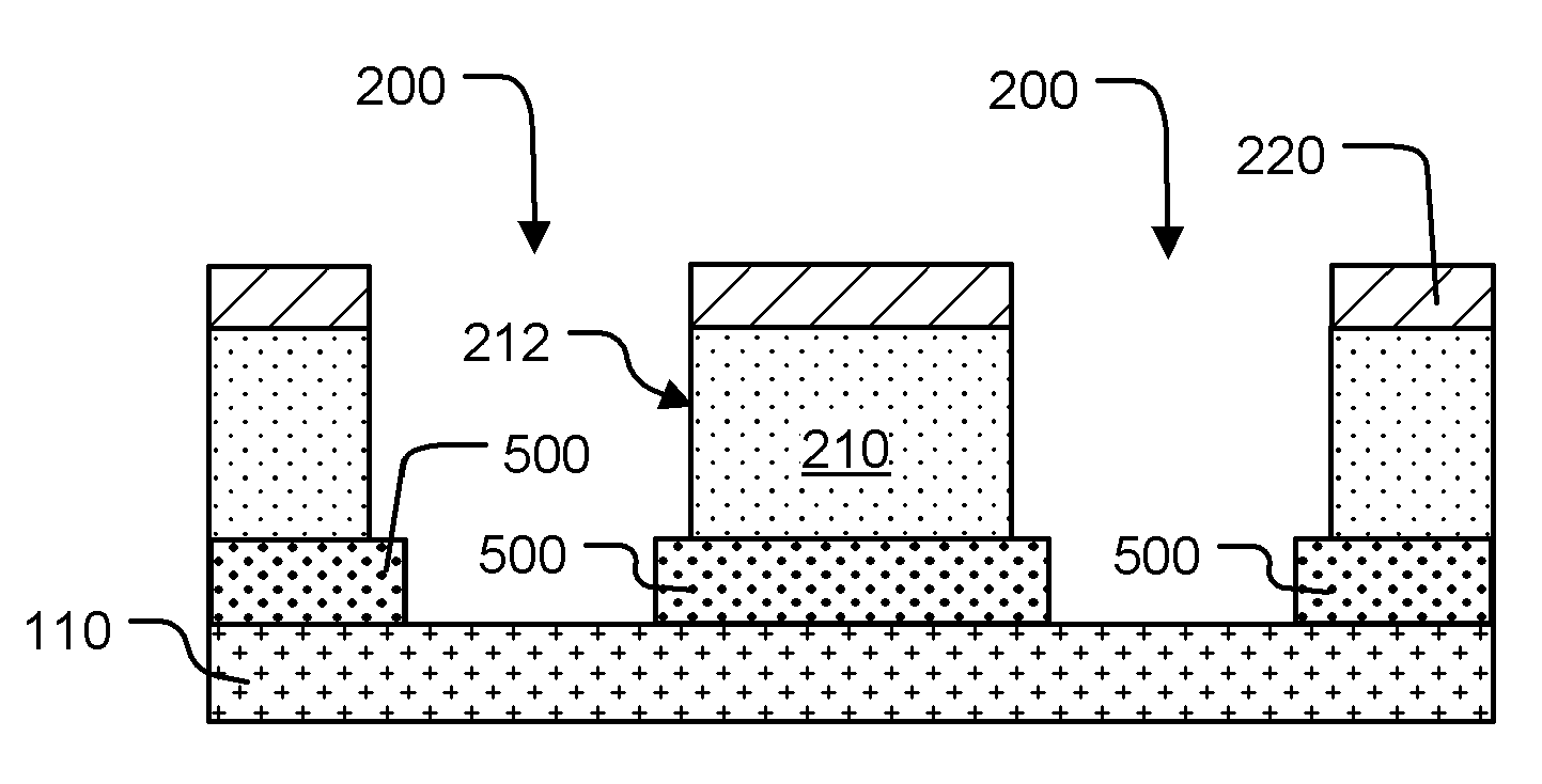
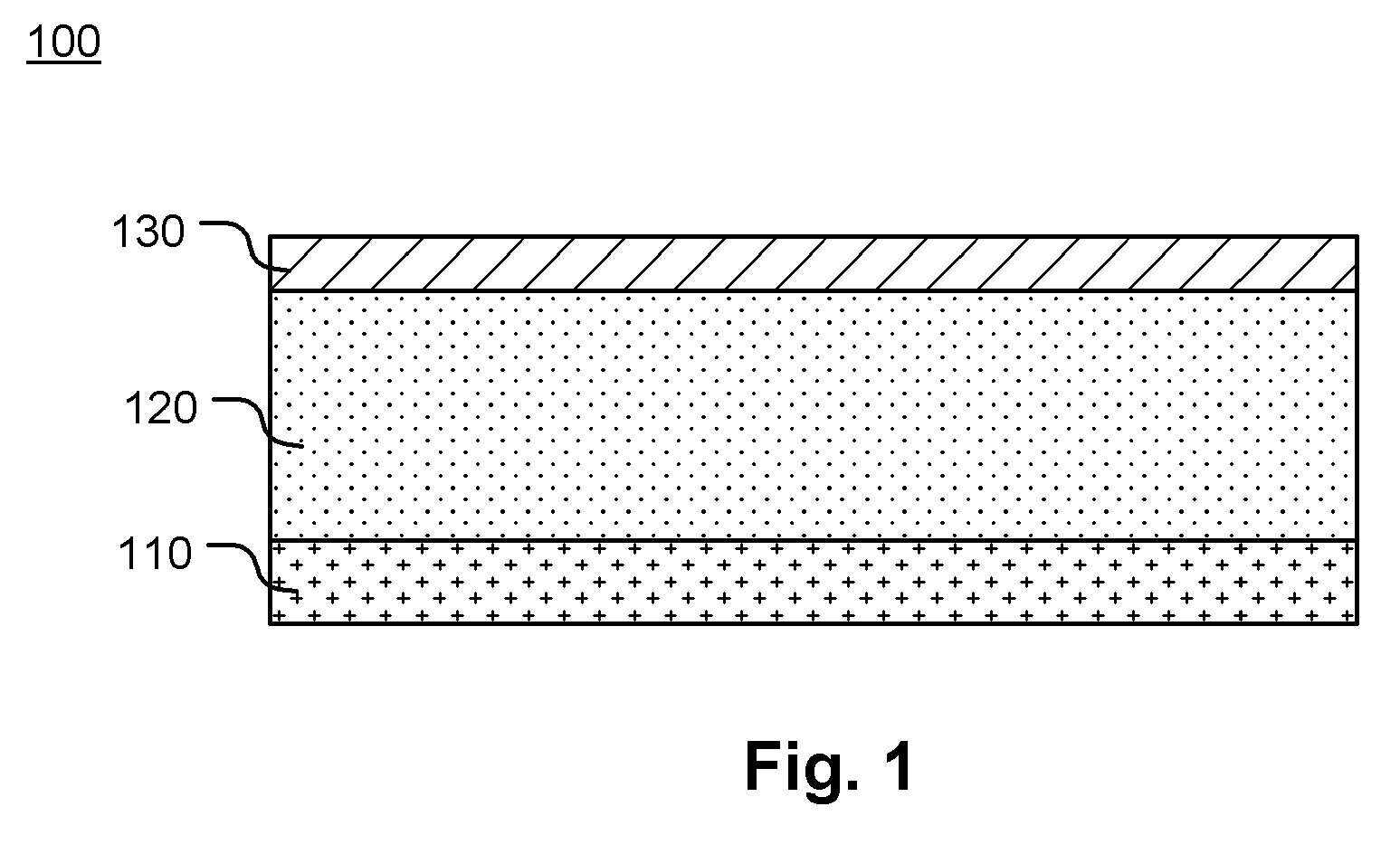
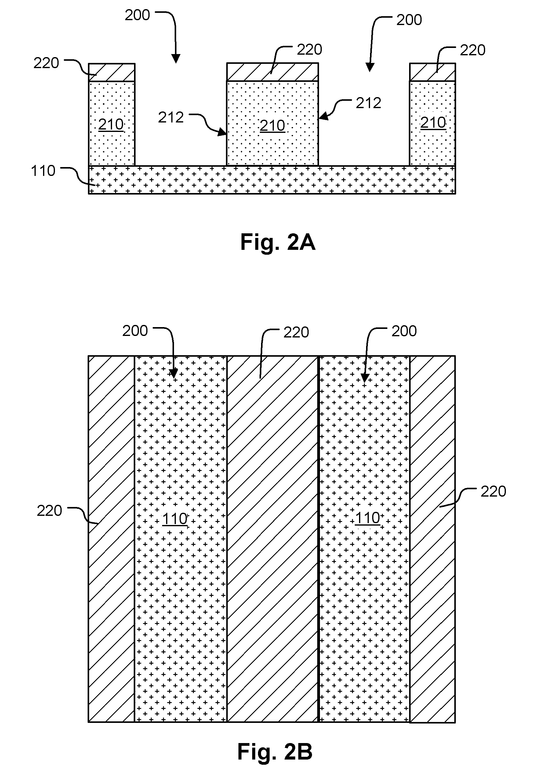
[0032]FIGS. 1-5 illustrate an embodiment of steps in a fabrication sequence for manufacturing buried silicide lines to reduce the loading effect of doped silicon material.
[0033]FIG. 1 illustrates a cross-sectional view of a step of forming a semiconductor body 100 by forming a layer of doped silicon 120 on an insulator layer 110, and forming a protection layer 130 on the layer of silicon 120. The layer of silicon 120 may be formed on the insulator layer 110, for example, using silicon-on-insulator techniques or the like. In the illustrated embodiment the insulator layer 110 comprises silicon dioxide.
[0034]The protection layer 130 can serve as an etch stop layer for the subsequent process steps described below. In the illustrated embodiment the protection layer 130 comprises silicon nitride. Alternatively, other materials may be used.
[0035]Next, a plurality of trenches 200 are formed through the protection layer 130 and the layer of silicon 120 to expose portions of the insulator lay...
PUM
 Abstract
Description
Claims
Application Information


