Display device and electronic apparatus

a display device and electronic equipment technology, applied in semiconductor devices, instruments, computing, etc., can solve the problems of deteriorating image quality and light-emission luminance changes, and achieve the effects of stabilizing signal writing time, suppressing the threshold voltage of sampling transistors, and stabilizing operation characteristics

Active Publication Date: 2012-05-01
JOLED INC
View PDF10 Cites 7 Cited by
  • Summary
  • Abstract
  • Description
  • Claims
  • Application Information

AI Technical Summary

Benefits of technology

[0014]There is a need for the present invention to provide a display device that can suppress change in the signal writing time. To meet this need, the following configuration is devised. Specifically, according to a mode of the present invention, there is provided a display device basically including a pixel array part and a drive part that drives the pixel array part. The pixel array part includes scan lines disposed along rows, signal lines disposed along columns, and pixels that are disposed at the intersections of the scan lines and the signal lines and are arranged in a matrix. The drive part includes a control scanner that sequentially applies a control pulse to the scan lines with a predetermined horizontal cycle to thereby line-sequentially scan the pixels on a row-by-row basis and a signal selector that supplies a video signal to the signal lines disposed along the columns in matching with the line-sequential scanning. The pixel includes a sampling transistor having a gate connected to the scan line and a source and a drain one of which is connected to the signal line, a drive transistor having a gate connected to the other of the source and the drain of the sampling transistor and a source and a drain one of which is connected to a power supply, a light-emitting element connected to the other of the source and the drain of the drive transistor, and a hold capacitor connected between the source and the gate of the drive transistor. The sampling transistor is kept at the on-state during the period from the rising of a control pulse supplied from the control scanner to the falling of the control pulse with a time width shorter than one horizontal cycle, and samples a video signal from the signal line to write the video signal to the hold capacitor. In addition, the sampling transistor has a double gate structure in which a pair of transistor elements are connected in series between the signal line and the gate of the drive transistor and the gates of the pair of transistor elements are connected in common. The drive transistor causes a drive current dependent on a video signal written to the hold capacitor to flow to the light-emitting element for light emission.
[0017]In the mode of the present invention, the sampling transistor has the double gate structure in which the pair of transistor elements are connected in series between the signal line and the gate of the drive transistor. Due to this feature, change in the threshold voltage of the sampling transistor can be suppressed compared with the case in which the double gate structure is not employed. Using the double gate structure stabilizes the operation characteristics and thus stabilizes the signal writing time, which depends on the width of the time during which the sampling transistor is kept at the on-state. Therefore, the change and lowering of the light-emission luminance do not occur, and therefore the image quality can be maintained.

Problems solved by technology

The change in the signal writing time leads to also change in the drive current supplied to the light-emitting element by the drive transistor, resulting in a problem that the light-emission luminance changes and the image quality is deteriorated.

Method used


Image

  • Display device and electronic apparatus
  • Display device and electronic apparatus
  • Display device and electronic apparatus

Examples


Embodiment Construction

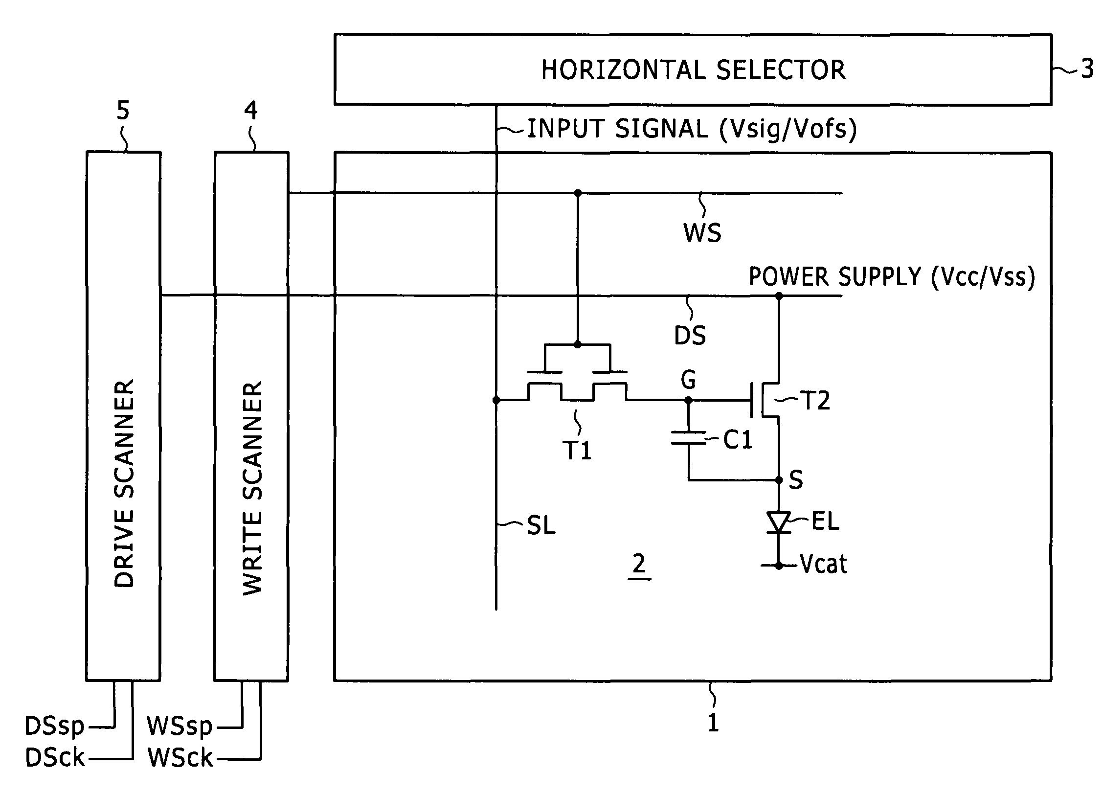
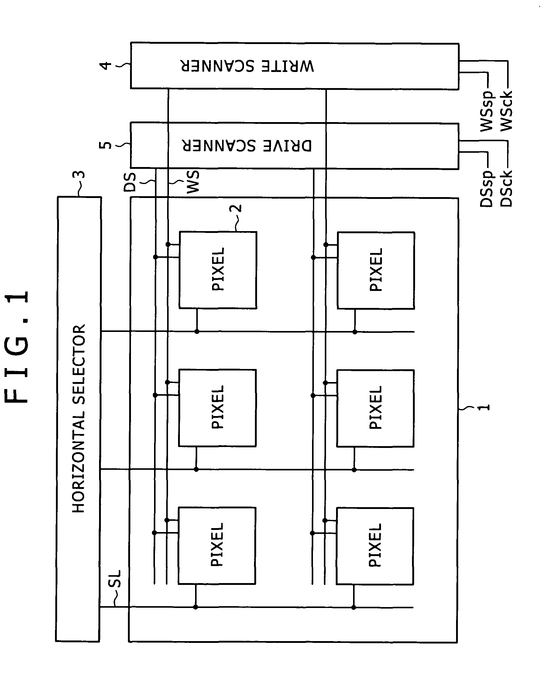
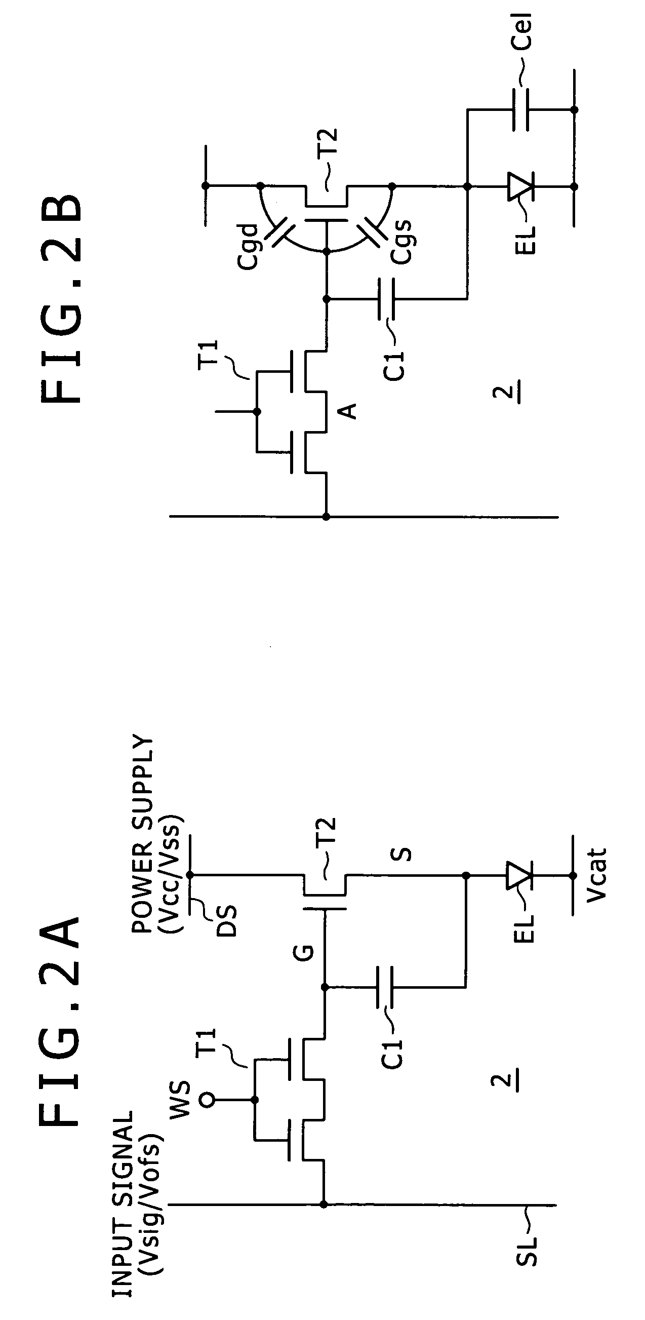
[0048]Embodiments of the present invention will be described in detail below with reference to the drawings. FIG. 1 is a block diagram showing the entire configuration of a display device according to the embodiments of the present invention. As shown in FIG. 1, this display device includes a pixel array part 1 and a drive part (3, 4, 5) for driving the pixel array part 1. The pixel array part 1 includes scan lines WS along the rows, signal lines SL along the columns, pixels 2 that are disposed at the intersections of both the lines and thus arranged in a matrix, and power feed lines DS disposed corresponding to the respective rows of the pixels 2. The drive part (3, 4, 5) includes a control scanner (write scanner) 4, a power supply scanner (drive scanner) 5, and a signal selector (horizontal selector) 3. The write scanner 4 sequentially supplies a control signal pulse to the respective scan lines WS to thereby line-sequentially scan the pixels 2 on a row-by-row basis. The drive sca...


PUM


Abstract

A sampling transistor in embodiments of the present invention is kept at the on-state with a time width shorter than one horizontal cycle, during the period from the rising of a control pulse supplied from a scanner to the falling of the control pulse, and samples a video signal Vsig from a signal line SL to write the video signal Vsig to a hold capacitor. A sampling transistor T1 has a double gate structure in which a pair of transistor elements are connected in common. This suppresses change in the threshold voltage of the sampling transistor.

Description

BACKGROUND OF THE INVENTION[0001]1. Field of the Invention[0002]The present invention relates to an active-matrix display device including light-emitting elements in its pixels. Furthermore, the present invention relates to electronic apparatus including such a display device. More specifically, the invention relates to a technique for stabilizing the operation of active elements formed in the pixels.[0003]2. Description of the Related Art[0004]In recent years, development of flat self-luminous display devices including organic EL devices as light-emitting elements is being actively promoted. The organic EL device is based on a phenomenon that an organic thin film emits light in response to application of an electric field thereto. The organic EL device can be driven by application voltage of 10 V or lower, and thus has low power consumption. Furthermore, because the organic EL device is a self-luminous element that emits light by itself, it does not need an illuminating unit and th...

Claims


Application Information

Patent Timeline
Patent Type & Authority Patents(United States)
IPC IPC(8): G09G5/00
CPCG09G3/3233H01L27/3262G09G2300/0852H10K59/1213
Inventor YAMAMOTO, TETSUROYAMASHITA, JUNICHIJINTA, SEIICHIROSUGIMOTO, HIDEKIUCHINO, KATSUHIDE
Owner JOLED INC
Why Eureka
Try Eureka