Error detection control system

a control system and error detection technology, applied in the field of error detection control system, can solve the problems of complex circuit structure of the circuit used for forming the value limited data to be programmed in the status area ws, and inconvenient use of techniques

Active Publication Date: 2012-05-08
SHARP KK
View PDF12 Cites 2 Cited by
  • Summary
  • Abstract
  • Description
  • Claims
  • Application Information

AI Technical Summary

Benefits of technology

[0018]In view of the above-mentioned problems, the present invention has been devised, and an object thereof is to provide an error detection control system for a nonvolatile memory, which can execute an overwriting process in accordance with characteristics and states of data, without making the sequence of the error detecting processes and the circuit structure complicated, while maintaining a certain degree of data reliability and anti-tampering characteristic.
[0036]In accordance with the IC card of the aforementioned aspect, since the error detection control system of any one of the first to eighth aspects is installed therein, it is possible to achieve all the functions and effects in the error detection control system in the first aspect. That is, in accordance with the IC card of the aforementioned aspect, it is possible to execute an error detecting process effective from the viewpoints of the data reliability and anti-tampering characteristic on read-out data on which no overwriting process is carried out or no overwriting process has been carried out, and it is also possible to execute an overwriting process effective from the viewpoint of a high-speed processing on read-out data on which an overwriting process is desirably carried out or an overwriting process has been executed; thus, an optimal process can be executed automatically depending on the data types and storage states.

Problems solved by technology

In the error detecting technique disclosed in Patent Document 1, however, it is necessary to program data that is consistent with the values already programmed in the main data area WM and the redundant data area WP, in the status area WS, with the result that the values of data to be programmed in the status area WS are limited.
Moreover, in the error detecting technique described in Patent Document 1, the value to be programmed in the status area WS is limited, and since it is difficult to execute so-called overwriting processes a plurality of times, this technique is not suitable for use in data on which, like the aforementioned program counter data, overwriting processes of a plurality of times are preferably carried out.
Moreover, in the error detecting technique described in Patent Document 1, since it is necessary to program data that is consistent with the values already programmed in the main data area WM and the redundant data area WP in the status area WS, the circuit used for forming the value to be programmed in the status area WS tends to have a complex circuit structure.
That is, as these areas increase, the amount of data required for the data area increases to cause the necessity of having to increase the storage area in the flash memory by a corresponding amount.

Method used


Image

  • Error detection control system
  • Error detection control system
  • Error detection control system

Examples


first embodiment

[0075]Referring to FIGS. 1 to 6, the following description will discuss a first embodiment of the present inventive system. In the present embodiment, the explanation is given on the assumption that the present inventive system is installed on an IC card.

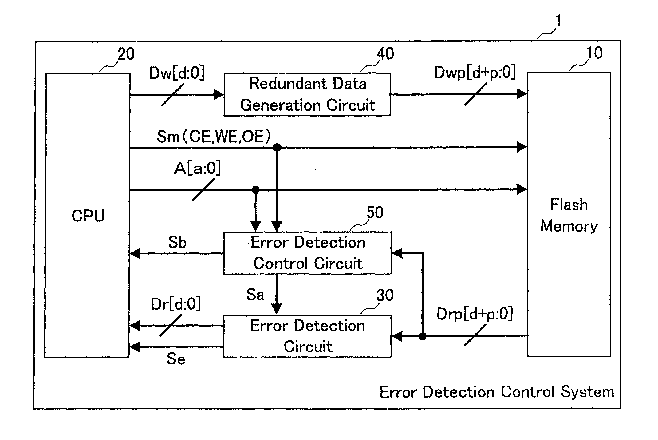
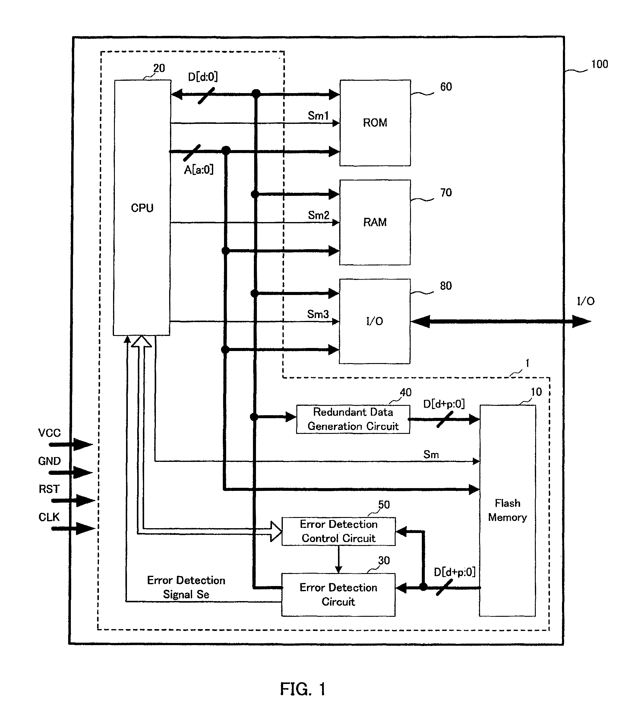
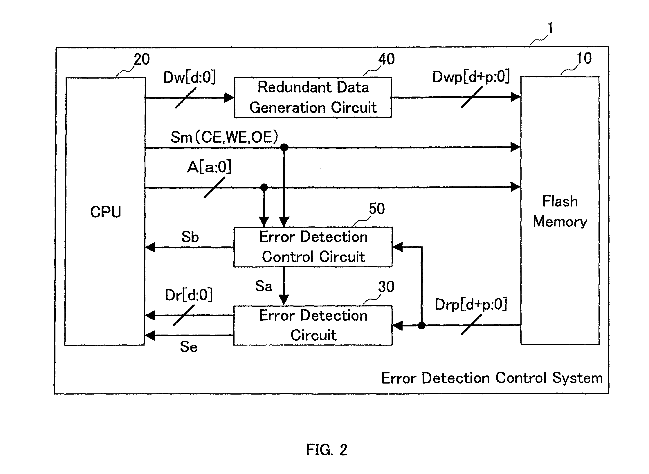
[0076]First, referring to FIGS. 1 to 5, the following description will discuss the structures of the present inventive system and IC card of the present embodiment. In this case, FIG. 1 shows a schematic structural example of an IC card 100 on which a present inventive system 1 has been installed, and FIG. 2 shows a schematic structural example of the present inventive system 1 of the present embodiment.

[0077]As shown in FIG. 1, the present inventive system 1 of the present embodiment is mounted on the IC card 100, and the IC card 100 is configured by a flash memory 10, a CPU (central processing unit) 20, an error detection circuit 30, a redundant data generation circuit 40 and an error detection control circuit 50 that constitute t...

second embodiment

[0109]Referring to FIG. 7, the following description will discuss the present inventive system 1 in accordance with the second embodiment. The present embodiment differs from the first embodiment in that the determining method for the data type of read-out data is made different. More specifically, in the first embodiment, the data type is determined based upon the address map of the flash memory 10; however, in the present embodiment, the data type is determined based upon an error detection control signal Sc from the CPU 20.

[0110]Referring to FIG. 7, the following description will discuss the structure of the present inventive system 1 in accordance with the present embodiment. As shown in FIG. 7, the present inventive system 1 in accordance with the present embodiment is configured by a flash memory 10, a CPU 20, an error detection circuit 30, a redundant data generation circuit 40 and an error detection control circuit 50, and the structures of the flash memory 10, the error det...

third embodiment

[0114]Referring to FIG. 8, the following description will discuss the present inventive system 1 in accordance with the third embodiment. In the present embodiment, an explanation will be given to a system in which the setting method of the availability of the error detecting process is different from those of the first and second embodiments. More specifically, in the first and second embodiment, the availability of the execution of the error detecting process is set based upon the data type of the read-out data; however, the availability of the execution of the error detecting process is set based upon a storage state that indicates whether an overwriting process has been executed or not.

[0115]Referring to FIG. 8, the following description will discuss the structure of the present inventive system 1 in accordance with the present embodiment. As shown in FIG. 8, the present inventive system 1 in the present embodiment is configured by a flash memory 10, a CPU 20, an error detection...


PUM


Abstract

An error detection control system for a nonvolatile memory comprises: a nonvolatile memory having data areas for a plurality of addresses each including a main data area and a redundant data area for one address; memory control means for controlling on the nonvolatile memory a batch erasing process on a data area group basis, a reading process on the data area basis, a programming process on the data area basis, and an overwriting process on a bit basis; error detecting means for executing the error detecting process based upon the corresponding redundant data; error detecting control means for controlling availability of execution of the error detecting process based upon data types to be classified depending on whether or not the data is subjected to the overwriting process or a storage state indicating whether or not the overwriting process has been executed.

Description

CROSS-REFERENCE TO RELATED APPLICATIONS[0001]This application is a National Phase filing under 35 U.S.C. §371 of International Application No. PCT / JP2008 / 054570 filed on Mar. 13, 2008, and which claims priority to Japanese Patent Application No. 2007-098800 filed on Apr. 4, 2007.TECHNICAL FIELD[0002]The present invention relates to an error detection control system for a semiconductor device provided with a nonvolatile memory, and more particularly concerns an error detection control system including a nonvolatile memory provided with data areas for a plurality of addresses each configured by a main data area and a redundant data area, memory control means for controlling to the nonvolatile memory a batch erasing process on a data area group basis, a reading process on a data area basis, a programming process on the data area basis and an overwriting process on a bit basis, and error detection means for executing an error detecting process on the read-out data based upon the corresp...

Claims


Application Information

Patent Timeline
Patent Type & Authority Patents(United States)
IPC IPC(8): G11C29/00G06F11/00H03M13/00G06F21/75G06F21/86
CPCG06F11/1068
Inventor OHYAMA, SHIGEO
Owner SHARP KK
Why Eureka
Try Eureka