Array type chip resistor

a chip resistor and array technology, applied in the manufacture of resistor chips, resistor details, envelope/housing resistors, etc., can solve the problems of conventional chip resistors with a variety of quality problems, the size of personal computers and servers gradually becoming small, and the limit of downsizing the semiconductor modules mounted on the pcs or servers, etc., to prevent the resistive element from being damaged.

Active Publication Date: 2012-05-15
SAMSUNG ELECTRO MECHANICS CO LTD
View PDF16 Cites 15 Cited by
  • Summary
  • Abstract
  • Description
  • Claims
  • Application Information

AI Technical Summary

Benefits of technology

[0013]The present invention has been proposed in order to overcome the above-described problems and it is, therefore, an object of the present invention to provide an array type chip resistor, in which a resistive element is disposed below a substrate so that a resistive element can be prevented from being exposed to outside when the resistive element is mounted, which results in preventing the resistive element from being damaged due to external impact.
[0014]Further, another object of the present invention is to provide an array type chip resistor which can prevent short generation due to scratch by minimizing areas of upper electrodes and side electrodes exposed to outside of the substrate.
[0022]Also, the plating layer performs protection of the lower electrodes, as well as formation of external electrodes by growing Ni—Sn plating layer on the leveling electrodes so that it can be exposed to outside of the chip resistor.
[0023]Also, the chip resistor may further include an insulating layer which covers outside of the protection layer, and the insulating layer is made of polymer and finally protects the resistive element. Further, the insulating layer prevents plating solution from infiltrating to the resistive element when the plating layer for formation of the external electrode is formed.

Problems solved by technology

The sizes of personal computers (PC) and servers gradually become small, but there is a limit in downsizing the semiconductor module mounted on the PCs or servers, e.g., memory module.
However, it have been pointed out that the conventional chip resistor has a variety of quality problems due to external environment when mounted on a printed circuit board.
When mounted on a PCB or moved for mounting, the conventional chip resistor has problems of damages of the substrate and corners thereof due to external impact by worker's carelessness.
Further, when external impact is applied to the resistive element exposed to the top surface of the substrate during mounting, the resistive element may be damaged.
In the conventional chip resistor, there may be produced scratch phenomenon that peels coating materials of an external electrode printed on side surfaces thereof due to external friction or contact between chip resistors.
Further, there may be also produced short between electrodes due to the scratch phenomenon when soldering is performed for mounting the chip resistor.
However, the bearing layer is insufficient for prevention of electrode short.

Method used


Image

  • Array type chip resistor
  • Array type chip resistor
  • Array type chip resistor

Examples


Embodiment Construction

[0038]An array type chip resistor in accordance with the present invention will be described in detail with reference to the accompanying drawings. When describing them with reference to the drawings, the same or corresponding component is represented by the same reference numeral and repeated description thereof will be omitted.

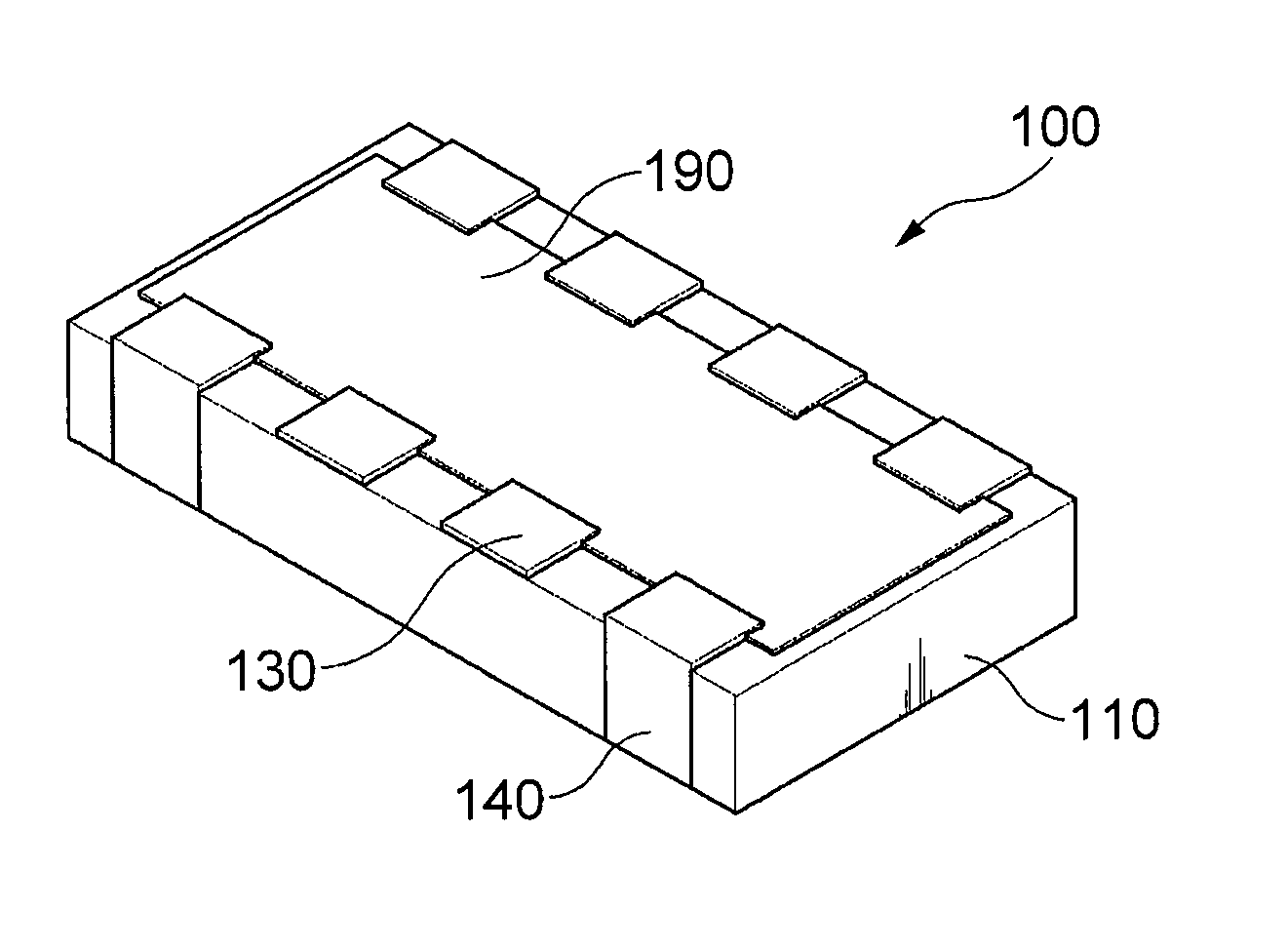
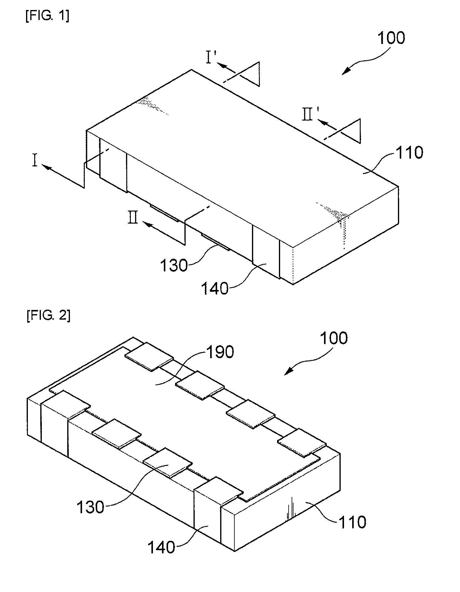
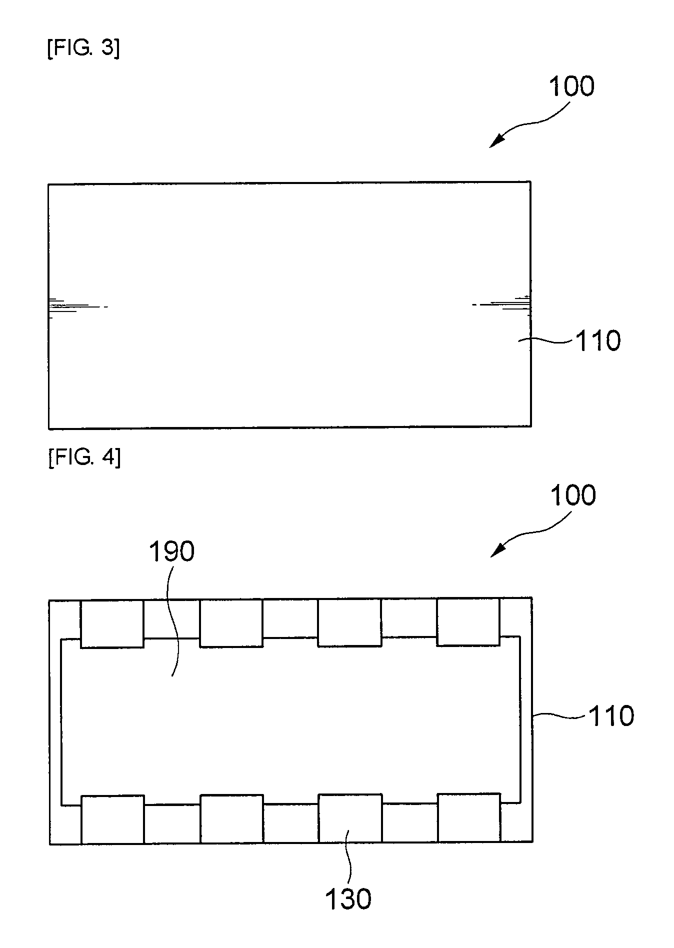
[0039]FIG. 1 is a perspective view showing a chip resistor in accordance with one embodiment of the present invention. FIG. 2 is a bottom perspective view showing a chip resistor in accordance with one embodiment of the present invention. FIG. 3 is a plane view showing a chip resistor in accordance with one embodiment of the present invention. FIG. 4 is a rear view showing a chip resistor in accordance with one embodiment of the present invention. FIG. 5 is a cross-sectional view taken along I-I′ and II-II′ of FIG. 1.

[0040]As shown in drawings, the chip resistor 100 in accordance with one embodiment of the present invention includes a substrate 110 having a ...


PUM


Abstract

The present invention provides an array type chip resistor including: a substrate formed in a rectangular parallelepiped shape; lower electrodes disposed on both sides of a bottom surface of the substrate at equal spaces; side electrodes extended from some of lower electrodes, formed on outermost edges of both sides of the substrate, in all lower electrodes, to a side surface of the substrate; a resistive element interposed between lower electrodes of the bottom surface of the substrate; a protection layer covered on the resistive element, the protection layer having both sides which cover a part of the lower electrodes and the resistive element; leveling electrodes being in contact with the lower electrodes exposed to outside of the protection layer; and a plating layer formed on the leveling electrodes. The array type chip resistor can prevent the resistive element from being damaged due to external impact when mounted since the resistive element is printed inside of the lower electrodes of the bottom surface of the substrate.

Description

CROSS-REFERENCE TO RELATED APPLICATIONS[0001]This application claims the benefit of Korean Patent Application Nos. 10-2009-0083519 and 10-2009-0083521 filed with the Korea Intellectual Property Office on Sep. 4, 2009, the disclosures of which are incorporated herein by references.BACKGROUND OF THE INVENTION[0002]1. Field of the Invention[0003]The present invention relates to an array type chip resistor; and, more particularly, to an array type chip resistor, in which a resistor element is disposed below a substrate so that the resistor element can be prevented from being damaged due to external impact.[0004]2. Description of the Related Art[0005]In general, a chip resistor refers to a resistor manufactured in a semiconductor package type by mounting a number of resistors into one body so as to increase a degree of integration of electronic products.[0006]Such a chip resistor is mostly mounted on a semiconductor module. The sizes of personal computers (PC) and servers gradually becom...

Claims


Application Information

Patent Timeline
Patent Type & Authority Patents(United States)
IPC IPC(8): H01C1/012
CPCH01C1/034H01C1/14H01C17/006H01C17/02
Inventor RYU, HEUNG BOKPARK, JANG HOKIM, YOUNG KEYSUH, KI WONCHOI, YUN GAB
Owner SAMSUNG ELECTRO MECHANICS CO LTD
Why Eureka
Try Eureka