Circuit with transistors integrated in three dimensions and having a dynamically adjustable threshold voltage VT

a technology of three-dimensional circuits and transistors, applied in the field of microelectronics, can solve the problems of reducing the supply voltage below a value around 3 times the threshold voltage of the transistors, affecting the operation speed, and affecting the signal propagation time,

Active Publication Date: 2012-05-22
COMMISSARIAT A LENERGIE ATOMIQUE ET AUX ENERGIES ALTERNATIVES
View PDF18 Cites 207 Cited by
  • Summary
  • Abstract
  • Description
  • Claims
  • Application Information

AI Technical Summary

Benefits of technology

[0052]The coupling may be such that a variation in the gate potential of the first transistor of at the most Vdd (where Vdd is a supply voltage of the device) makes it possible to obtain a variation in the threshold voltage of the second transistor of at least 50 mV.
[0054]The thickness as well as the dielectric materials of the insulating zone may also be chosen to make it possible to prevent a coupling between the access zones of the first transistor and those of the second transistor.
[0071]Such a layout can make it possible to reduce the topography of the gate and enable the impact of an involuntary misalignment between the upper and lower gate to be reduced.

Problems solved by technology

However, a reduction in the supply voltage below a value around 3 times the threshold voltage of the transistors is likely to degrade in a significant manner the operating speed of said transistors.
But a reduction in the threshold voltage has a tendency to bring about an increase in the static consumption.
Such a structure has a high capacitance between the source and drain zones and the substrate, which has a tendency to induce a degradation of the signal propagation times.
The layout of the device is such that it poses problems of planeness and that a parasite electrical coupling can be established between the access zones of the first transistor and the second transistor, which has a tendency to reduce the operating speed of the device.

Method used


Image

  • Circuit with transistors integrated in three dimensions and having a dynamically adjustable threshold voltage VT
  • Circuit with transistors integrated in three dimensions and having a dynamically adjustable threshold voltage VT
  • Circuit with transistors integrated in three dimensions and having a dynamically adjustable threshold voltage VT

Examples


first embodiment

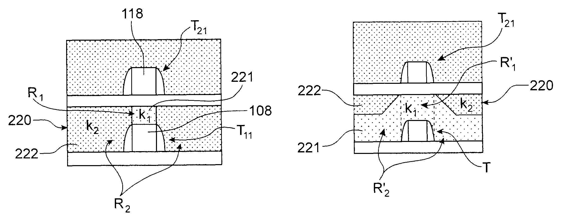
[0211]A first embodiment is given in FIG. 17, wherein the gate 108 of the first transistor T11 and the channel zone 116 of the second transistor T21 are separated by a first dielectric material 221 having a first dielectric constant k1.

[0212]On either side of this first region R1, above source and drain regions of the first transistor T11, the insulating zone 220 is formed based on a second dielectric material 222 having a second dielectric constant k2, such that k21. The first region R1 may be filled with a “high-k” dielectric material such as for example HfO2 of thickness for example around 40 nanometres, whereas the region situated around this first region may be filled with a dielectric material of thickness for example around 100 nanometres, of lower dielectric constant, such as SiO2.

[0213]With such a device, as a function of the manner in which the polarisation of the gate 108 of the first transistor T11 is provided, the threshold voltage VT of the channel of the second transi...

second embodiment

[0216]A second embodiment is given in FIG. 18. As in the example described previously in reference to FIG. 17, this device comprises an insulating zone 220 separating the transistors T11 and T21, formed of several different dielectric materials 221, 222, and in which the thickness and the composition vary depending on the region in which one is situated between the transistors T11 and T21.

[0217]The gate 108 of the first transistor T11 and the channel zone 116 of the second transistor T21 are separated by a first region R1 based on a first dielectric material 221, for example a dielectric material having a first dielectric constant k1. Around this first region R1, in a region R2 situated above source and drain regions of the first transistor T11 are provided insulating blocks formed of a stack of the first dielectric material 221 and a second dielectric material 222 having a second dielectric constant k2, such that k21. The first dielectric region R1 of the zone 220 thus has, by virt...


PUM


Abstract

A microelectronic device including: a substrate surmounted by a stack of layers, at least one first transistor situated at a given level of said stack, at least one second transistor situated at a second level of said stack, above said given level, the first transistor including a gate electrode situated opposite a channel zone of the second transistor, the first transistor and the second transistor being separated by an insulating zone, and said insulating zone being constituted of several different dielectric materials include a first dielectric material and a second dielectric material.

Description

TECHNICAL FIELD[0001]The present invention relates to the field of microelectronics and in particular that of devices comprising transistors distributed over several levels.[0002]It relates to the formation of a microelectronic device provided with transistors integrated in 3 dimensions and means for modulating the threshold voltage of transistors by coupling by means of the gate of lower level transistors.[0003]It brings improvements, particularly in terms of size, electrical performance, operating speed, and makes it possible to modify in a dynamic manner the threshold voltage of some of the transistors of the device, and to reduce the short channel effects of these transistors.[0004]The invention applies in particular to the field of random access memories, such as SRAM memories (SRAM for “static random access memory”).STATE OF THE PRIOR ART[0005]Generally speaking, increasing the density of components in microelectronic devices is a continual aim.[0006]To do this, among a consid...

Claims


Application Information

Patent Timeline
Patent Type & Authority Patents(United States)
IPC IPC(8): H01L29/66H01L29/94
CPCH01L27/11H01L27/1203H01L27/1108H01L27/1104H01L27/0688H10B10/125H10B10/00H10B10/12
Inventor BATUDE, PERRINECLAVELIER, LAURENTJAUD, MARIE-ANNETHOMAS, OLIVIERVINET, MAUD
Owner COMMISSARIAT A LENERGIE ATOMIQUE ET AUX ENERGIES ALTERNATIVES
Why Eureka
Try Eureka