Device for and a method of generating signals

a technology of a signal and a device, applied in the field of devices for generating signals, can solve the problems of inability to meet the requirements of silicon semiconductor technology, the maturity of this technology is still in its infancy, and the frequency generation limit of the semiconductor device is in the hundreds of ghz, etc., to achieve the effect of high frequency generation, simple measures, and high frequency components

Inactive Publication Date: 2012-05-22
NXP BV
View PDF6 Cites 3 Cited by
  • Summary
  • Abstract
  • Description
  • Claims
  • Application Information

AI Technical Summary

Benefits of technology

[0010]According to another exemplary embodiment of the invention, a method of generating an output signal having an increased output frequency compared to an input frequency of an input signal is provided, the method comprising providing a bipolar transistor having a base, a collector, and an emitter, controlling application of the input signal to the base, and controlling application of a collector-emitter voltage between the collector and the emitter in a manner for operating the bipolar transistor in a snap-back regime to obtain a non-linear collector current characteristic to thereby generate the output signal having the increased output frequency resulting from a steeply rising collector current.
[0018]By applying a sequence of input signals each having an input frequency (or a sufficiently narrow frequency distribution), a (quasi-)continuous production of very high frequencies can be achieved, that is to say with a forced repetitive event triggered by the application of the input signals and the biasing of the bipolar transistor terminals. Thus, embodiments of the invention may allow using a bipolar device in a very weird way that can be obtained with simple measures even in silicon technology.
[0019]Thus, embodiments of the invention do not have to rely on band diagrams (which limit available frequency values), and therefore do not require complex band engineering. Even direct band gaps are not required for embodiments of the invention. In contrast to this, a bipolar device is operated in a very uncommon way (particularly to repetitively trigger snap-back) to obtain a sharp rise of a transistor signal in the time domain, and consequently high frequency components at the Fourier transformed spectrum in the frequency domain. A device according to an exemplary embodiment of the invention may be denoted as a multiplier, which emits a high frequency signal at an output upon application of a lower frequency signal at an input.
[0020]More particularly, a very high frequency source (millimeter waves, terahertz) may be provided based on a standard semiconductor device or small circuit that enables a very high frequency generation by correctly tuning external components. The device may exploit the terminal instability mechanisms of bipolar devices. More particularly, embodiments of the invention use the electrothermal instability mechanism in standard silicon based bipolar devices to generate very high frequency harmonics that can reach well into the mmW wavelength range and into the THZ frequency range. As a consequence, embodiments of the invention may circumvent many problems associated to conventional frequency generators such as incompatibility with silicon technologies, requirement of low temperature operation, low maturity of the technology, or complexity of implementation. In accordance with this, embodiments of the invention enable the generation of very high frequencies in a way compatible with silicon base line process technologies, compatible with room temperature operation (which is important for large volume applications), compatible with mature semiconductor processes, and easy to implement.
[0022]According to a further exemplary embodiment, the device for generating an output signal having substantially same or increased output frequency compared to an input frequency of an input signal comprises a control unit adapted as a feedback loop for controlling application of the input signal, wherein the input signal is derived from the output signal. In other words, an oscillator is provided to make use of the snap-back behaviour to enable an inductor-less single transistor oscillator, preferably in the GHz-range. The fundamentals for an oscillator are available in the snap-back effect where the hysteresis is in the output current-voltage relation. The hysteresis curve may be easily tunable by external resistors.
[0026]The output frequency may be at least 100 GHz, particularly at least 1 THz. Thus, the output frequency may lie in the so-called terahertz gap that is conventionally difficult to handle regarding the generation / emission of electromagnetic or electric signals. Embodiments of the invention allow closing the terahertz gap.

Problems solved by technology

Nevertheless, an upper limit usually associated to semiconductor devices in terms of frequency generation is in the hundreds of GHz.
However, these photonic devices are bulky, require cryogenic temperature, or are not compatible with the ubiquitous silicon semiconductor technologies.
The first type of devices using exotic semiconductors rely on the use of the new plasma wave theory, however, the maturity of this technology is still in its infancy and has not be demonstrated in silicon.
The second, based on B—Si only works at cryogenic temperature that makes its use impractical for widespread commercial applications.

Method used


Image

  • Device for and a method of generating signals
  • Device for and a method of generating signals
  • Device for and a method of generating signals

Examples


Embodiment Construction

[0050]The illustration in the drawing is schematically. In different drawings, similar or identical elements are provided with the same reference signs.

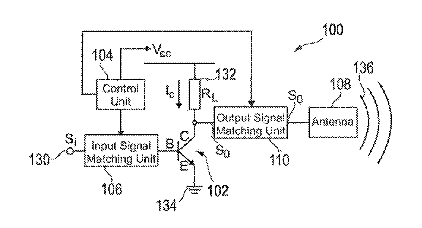
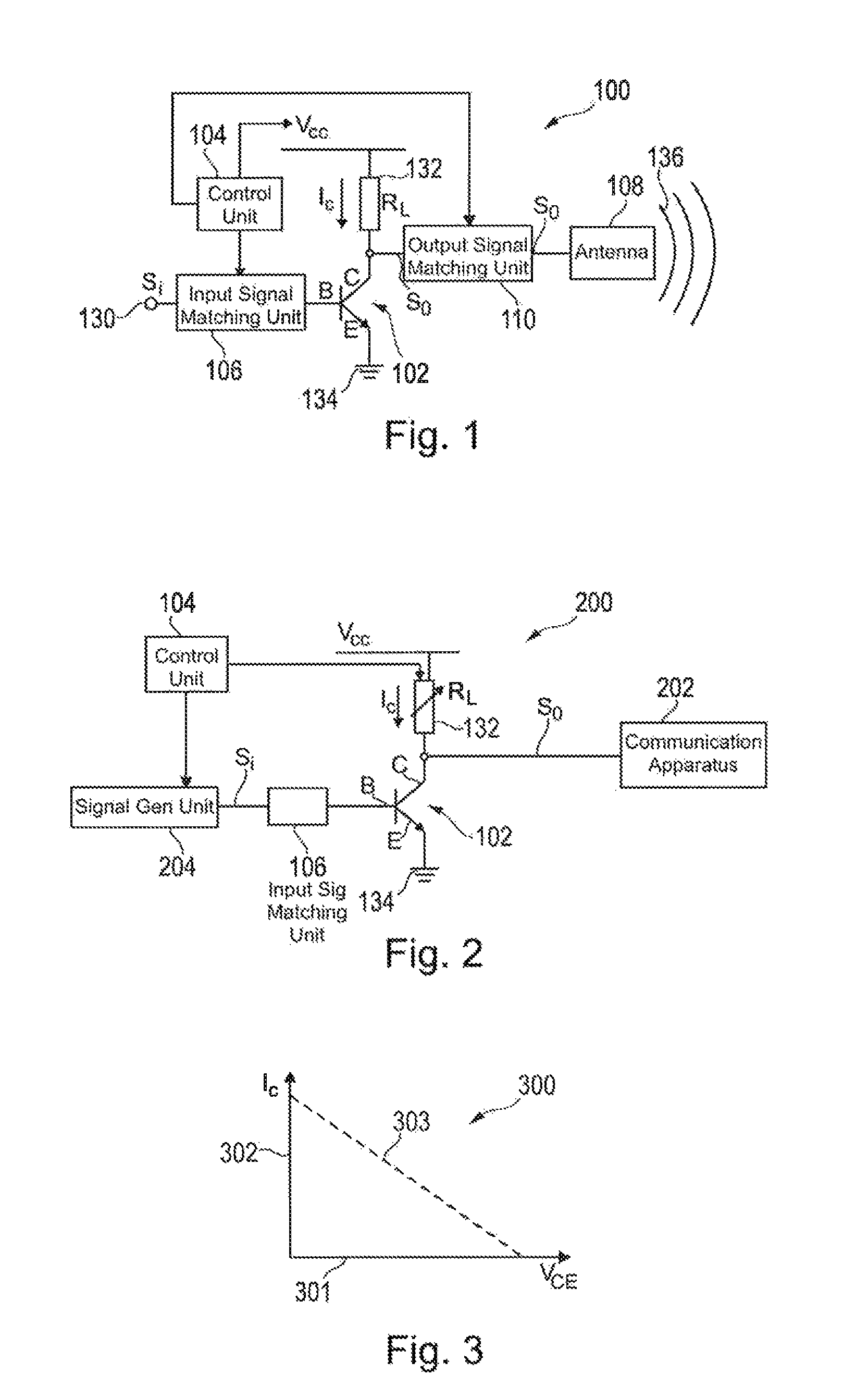
[0051]In the following, referring to FIG. 1, a device 100 for generating an output signal So having an increased output frequency compared to an input frequency of an input signal Si according to an exemplary embodiment of the invention will be explained.

[0052]A part or all of the components of the device 100 may be provided as a monolithically integrated semiconductor circuit.

[0053]The device 100 comprises a bipolar transistor 102 having a base B, a collector C and an emitter E.

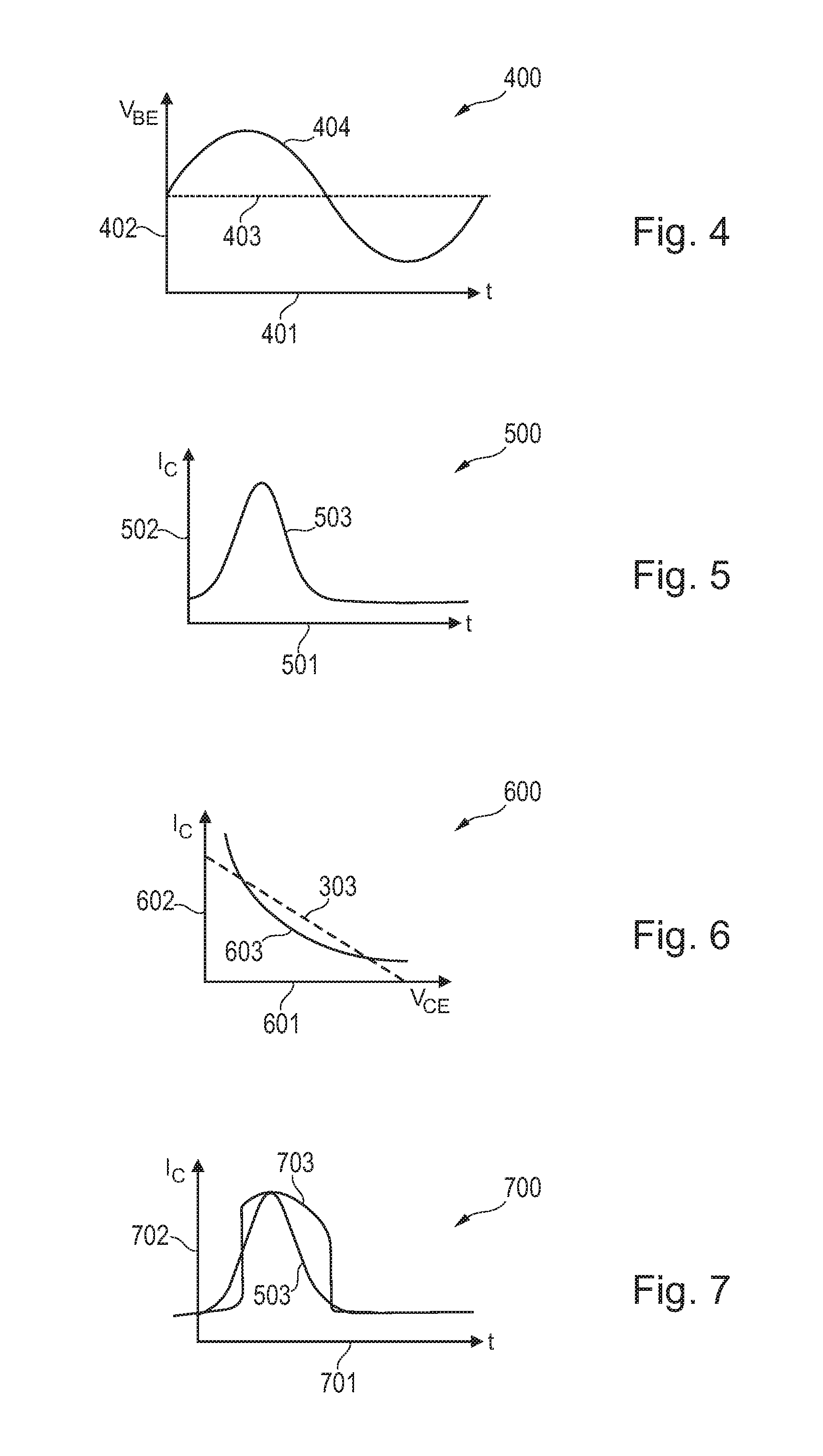
[0054]A control unit 104 is provided, which is adapted for controlling application of the input signal Si to the base B and which is adapted for controlling application of a collector-emitter voltage between the collector C and the emitter E in a manner for operating the bipolar transistor 102 in a snap-back regime (see FIG. 8) to obtain a non-linear collecto...


PUM


Abstract

A device (100) for generating an output signal (So) having substantially same or increased output frequency compared to an input frequency of an input signal (Si), the device (100) comprising: a bipolar transistor (102) having a base (B), a collector (C), and an emitter (E); a control unit (104) adapted for controlling application of the input signal (Si) to the base (B) and adapted for controlling application of a collector-emitter voltage between the collector (C) and the emitter (E) in a manner for operating the bipolar transistor (102) in a snap-back regime to obtain a non-linear collector current characteristic to thereby generate the output signal (So) having the substantially same or increased output frequency resulting from a steeply rising collector current.

Description

FIELD OF THE INVENTION[0001]The invention relates to a device for generating a signal. Beyond this, the invention relates to a method of generating a signal.BACKGROUND OF THE INVENTION[0002]A signal having a high frequency (from RF to THz) enables a wide variety of applications, ranging from gigabits / terabits bandwidth communication systems, to molecular analysis, and medical or industrial imaging.[0003]Known semiconductor devices enabling the generation of such signals having a high frequency include a Gunn diode, tunnelling diodes, transit time diodes, transistor (bipolar, FET)-based oscillators, and multiplier based oscillators relying on device non-linearities such as a Schottky diode.[0004]Nevertheless, an upper limit usually associated to semiconductor devices in terms of frequency generation is in the hundreds of GHz. As a consequence, photonic-based devices such as a gas laser, a quantum cascade laser, or photoconduction-based devices are serves in many applications requirin...

Claims


Application Information

Patent Timeline
Patent Type & Authority Patents(United States)
IPC IPC(8): H03B19/00
CPCH03B19/14H03F3/19H03D2200/0021
Inventor NUTTINCK, SEBASTIENVANHOUCKE, TONYHURKX, GODEFRIDUS
Owner NXP BV
Why Eureka
Try Eureka