PLD architecture optimized for 10G Ethernet physical layer solution

a physical layer and architecture technology, applied in the field of integrated circuit devices, can solve the problems of complex optical module connection to the plds, complex layout and interoperability, and small reduction of the complexity of the 10gbe implementation

Active Publication Date: 2012-05-22
ALTERA CORP
View PDF10 Cites 11 Cited by
  • Summary
  • Abstract
  • Description
  • Claims
  • Application Information

AI Technical Summary

Problems solved by technology

Even though this 10 GbE PHY layer implementation can be designed using available components, integrating such a PHY layer design within a system requires many components, uses a large amount of circuit board area, and creates potentially complex layout and interoperability issues.
However, these implementations do little to reduce the complexity of the 10 GbE implementations.
The large bus protocols that are needed to connect the optical modules to the PLDs are complex and lead to reduced performance.
Typically implementing these protocols within a PLD requires additional buffers, clock dividers, and reference clock signals which adds latency, timing constraints, and power consumption to the system.
Further, compared to ordinary optical transceivers, the optical modules that must be used in this implementation are expensive and have high power and space requirements.

Method used


Image

  • PLD architecture optimized for 10G Ethernet physical layer solution
  • PLD architecture optimized for 10G Ethernet physical layer solution
  • PLD architecture optimized for 10G Ethernet physical layer solution

Examples


Embodiment Construction

[0011]Although the invention is equally applicable to other types of integrated circuits (e.g., various kinds of programmable integrated circuits such as programmable microcontrollers, etc.), the invention will be fully understood from the following illustrative discussion of its application to the type of integrated circuits known as programmable logic devices (PLDs).

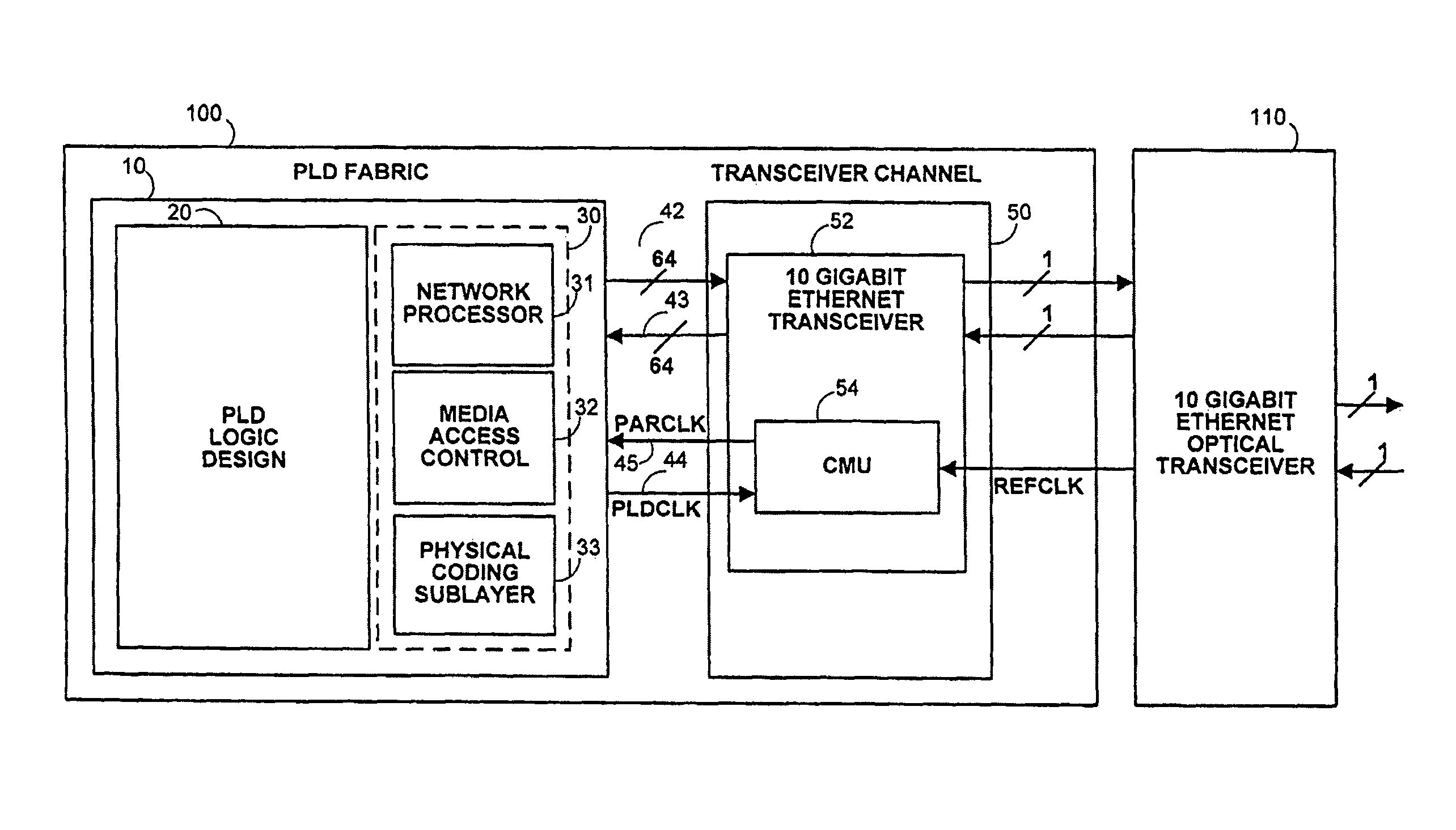
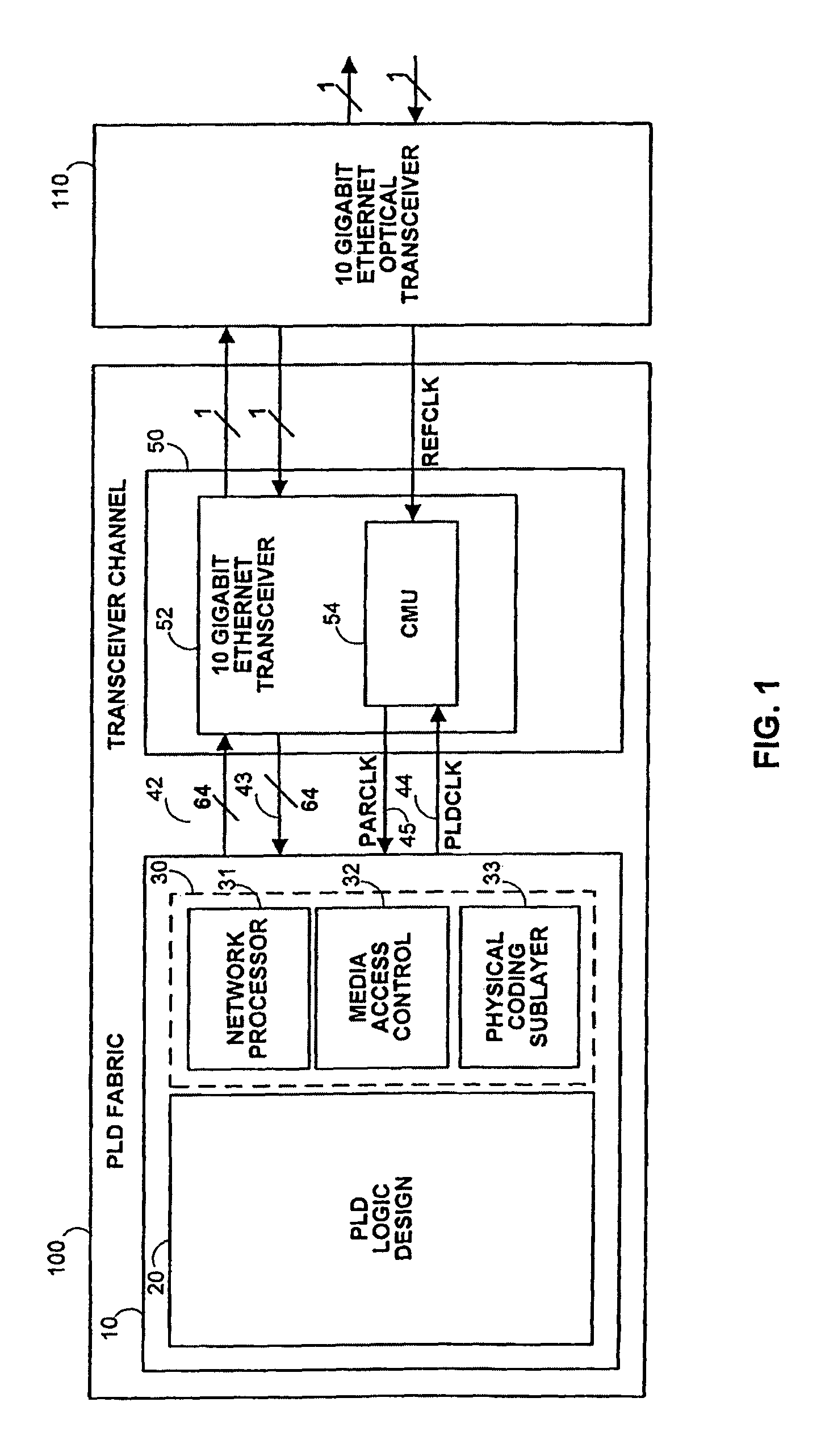
[0012]An illustrative embodiment of a 10 Gigabit Ethernet (10 GbE) physical (PHY) layer implemented within a PLD in accordance with the invention is shown in FIG. 1. As shown in FIG. 1, PLD 100 includes primarily general-purpose-programmable logic fabric 10 and transceiver channel 50. PLD 100 is connected to 10 GbE optical transceiver module 110 that coverts electrical 10 GbE signals into optical 10 GbE signals and vise versa. Thus, other than the optical-electrical conversion provided by 10 GbE optical transceiver module 110, all of the functions of the 10 GbE PHY layer may be implemented within PLD 100.
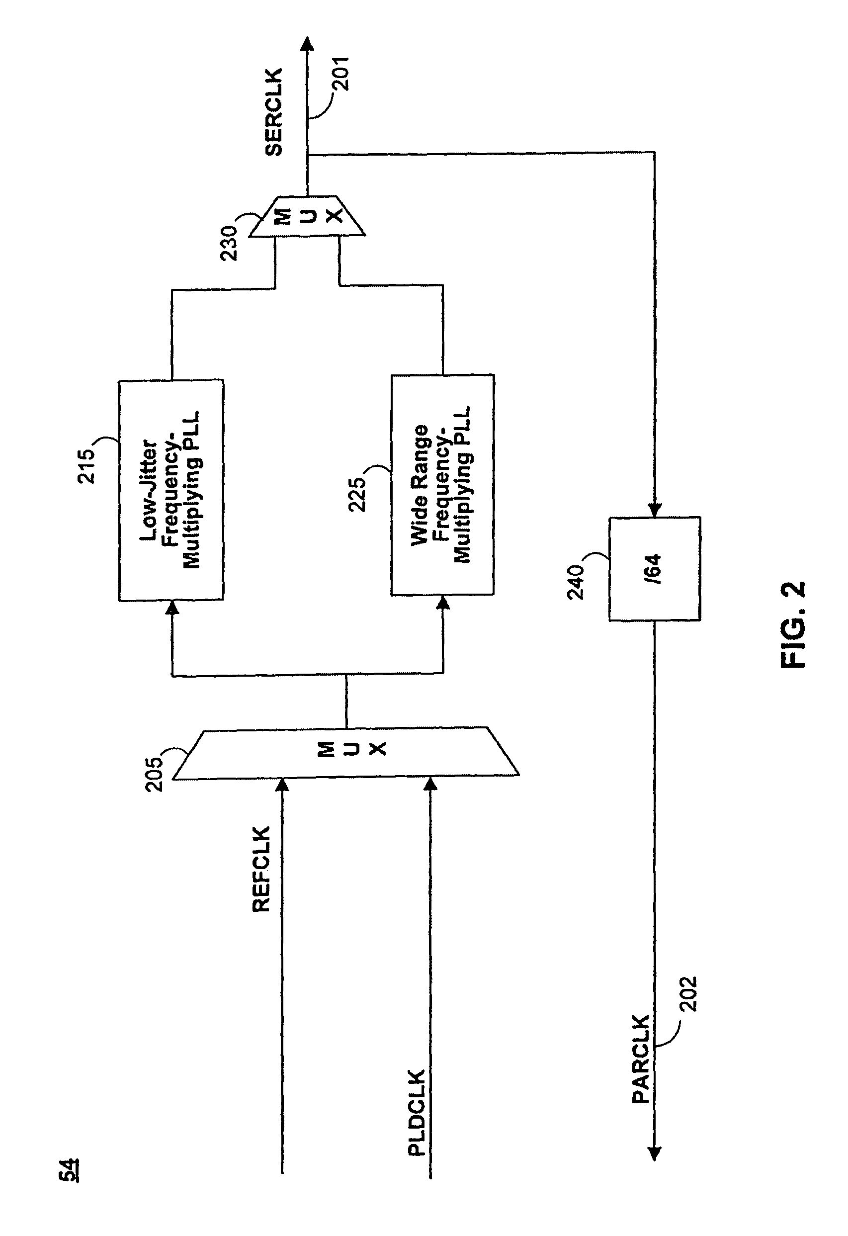
[0013]PLD fabr...


PUM


Abstract

An integrated circuit (e.g., a programmable integrated circuit such as a programmable microcontroller, a programmable logic device, etc.) includes programmable circuitry and 10 Gigabit Ethernet (10 GbE) transceiver circuitry. The programmable circuitry and the transceiver circuitry may be configured to implement the physical (PHY) layer of the 10 GbE networking specification. This integrated circuit may then be coupled to an optical transceiver module in order to transmit and receive 10 GbE optical signals. The transceiver circuitry and interface circuitry that connects the transceiver circuitry with the programmable circuitry may be hard-wired or partially hard-wired.

Description

BACKGROUND OF THE INVENTION[0001]This invention relates to integrated circuit devices, and more particularly to 10 Gigabit Ethernet (10 GbE) physical (PHY) layer circuitry for use in programmable integrated circuit devices.[0002]As the demand for network bandwidth increases, the adoption of 10 GbE is gaining a great deal of momentum for use in local area networks (LANs), wide area networks (WANs), and metropolitan area networks (MANs). 10 GbE is a version of Ethernet with a nominal data rate of 10 Gigabits per second and is specified by the IEEE 802.3ae standard. The IEEE 802.3ae standard is incorporated by reference herein in its entirety. Due to the high speed and demanding specifications of the 10 GbE standard, especially at the PHY layer, performance is a key differentiating factor between network equipment providers.[0003]The PHY layer of 10 GbE can be implemented by integrating a number of available components that communicate via standard interfaces. For example, a typical 10...

Claims


Application Information

Patent Timeline
Patent Type & Authority Patents(United States)
IPC IPC(8): H04L12/56
CPCH04L49/30H04L49/352
Inventor CHAN, ALLENSHUMARAYEV, SERGEYWONG, WILSONDING, WEIQI
Owner ALTERA CORP
Why Eureka
Try Eureka