Apparatus and method for uniform metal plating

a technology of uniform metal plating and uniform surface, applied in the direction of film/foil adhesives, tubular fabrics, shaping/stretching, etc., can solve the problems of affecting the overall process flow, increasing the time required for plating, and exacerbated issues associated with plating a uniform metal layer over features in various positions across a major surface of a substra

Active Publication Date: 2012-05-29
SKYWORKS SOLUTIONS INC
View PDF10 Cites 13 Cited by
  • Summary
  • Abstract
  • Description
  • Claims
  • Application Information

AI Technical Summary

Benefits of technology

[0008]One aspect of the disclosure is an apparatus for plating one or more features of a GaAs wafer with gold. The apparatus includes an anode and a showerhead body coupled to the anode. The anode includes an anode post and a showerhead anode plate. The anode post has at least one opening for providing a gold plating solution, and the showerhead anode plate has holes sized to dispense the gold plating solution onto the GaAs wafer. The showerhead body is coupled to the anode post and the showerhead anode plate. In addition, the showerhead body is configured to create a seal sufficient to substantially prevent a reduction of pressure in the gold plating solution flowing from the anode post and the holes of the showerhead anode plate.

Problems solved by technology

As wafer size increases, issues associated with plating a uniform metal layer over features in various positions across a major surface of a substrate may become exacerbated.
Moreover, the time required for plating may increase for larger wafers, slowing down the overall process flow.

Method used


Image

  • Apparatus and method for uniform metal plating
  • Apparatus and method for uniform metal plating
  • Apparatus and method for uniform metal plating

Examples


Embodiment Construction

[0029]The headings provided herein, if any, are for convenience only and do not necessarily affect the scope or meaning of the claimed invention.

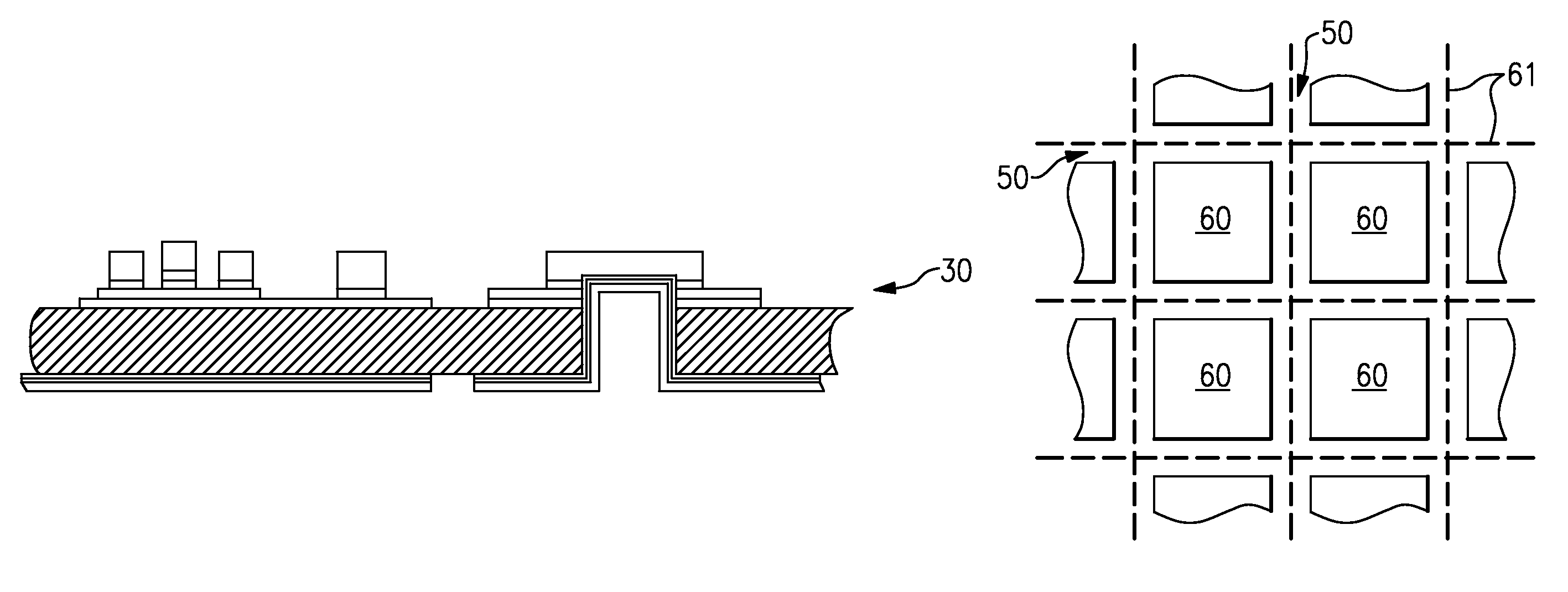
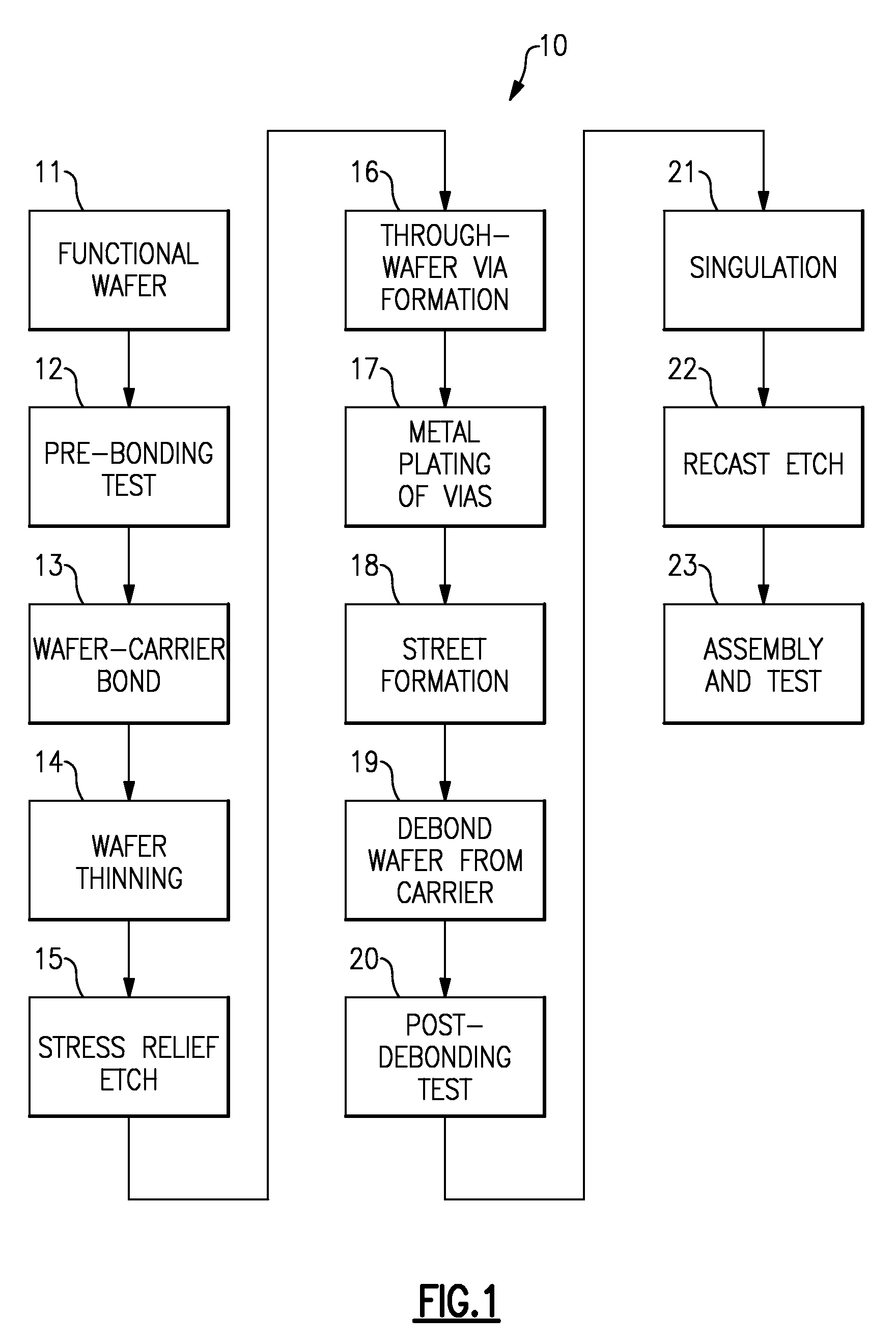
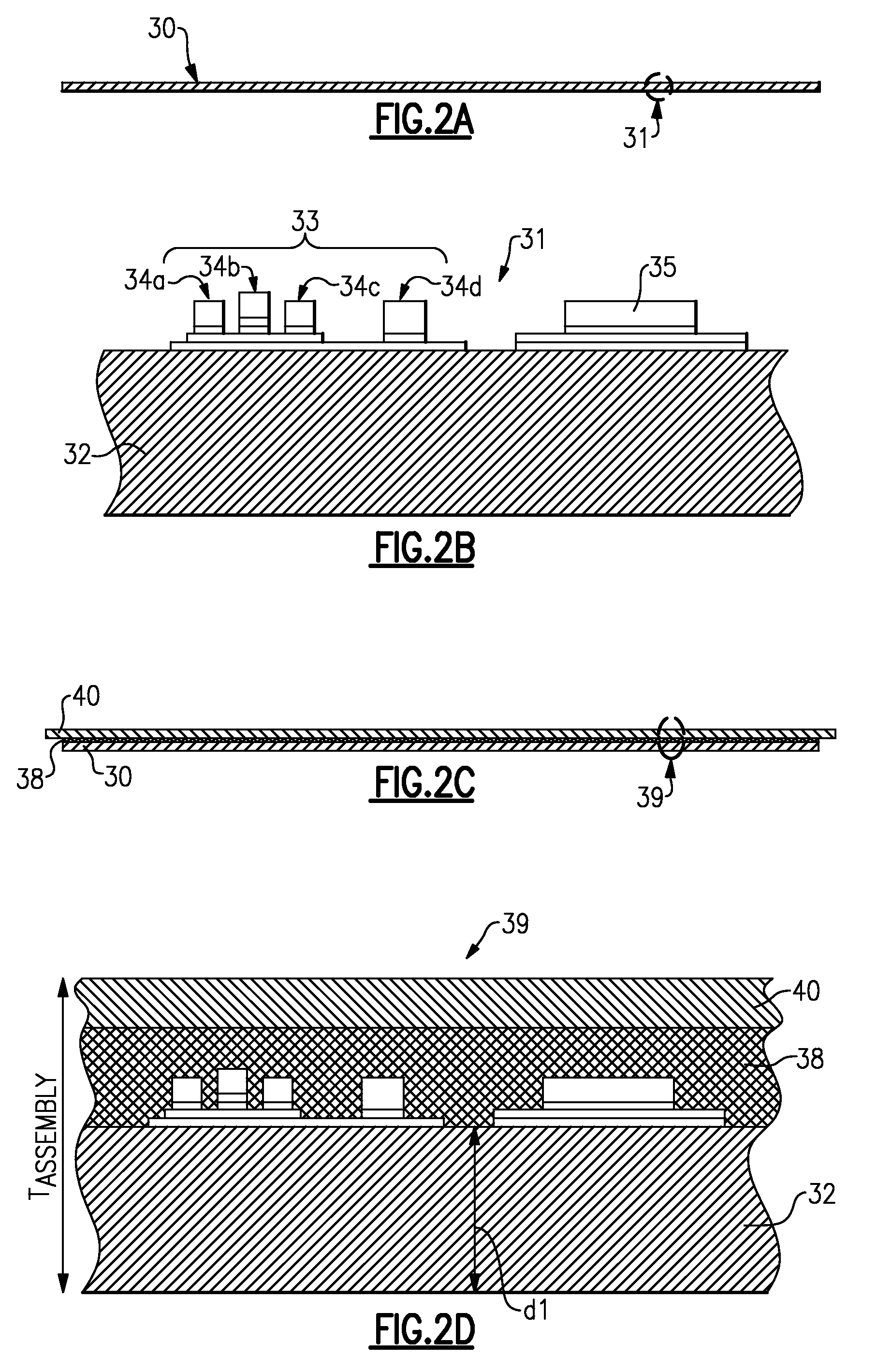
[0030]Provided herein are various methodologies and devices for processing wafers such as semiconductor wafers. FIG. 1 shows an example of a process 10 where a functional wafer is further processed to form through-wafer features such as vias and back-side metal layers. As further shown in FIG. 1, the example process 10 can include bonding of a wafer to a carrier for support and / or to facilitate handling during the various steps of the process, and debonding of the wafer from the carrier upon completion of such steps. FIG. 1 further shows that such a wafer separated from the carrier can be further processed so as to yield a number of dies.

[0031]In the description herein, various examples are described in the context of GaAs substrate wafers. It will be understood, however, that some or all of the features of the present disclosure can be imp...


PUM

PropertyMeasurementUnit
diameteraaaaaaaaaa
depthaaaaaaaaaa
diameteraaaaaaaaaa

Abstract

Apparatus and methods for uniform metal plating onto a semiconductor wafer, such as GaAs wafer, are disclosed. One such apparatus can include an anode and a showerhead body. The anode can include an anode post and a showerhead anode plate. The showerhead anode plate can include holes sized to dispense a particular plating solution, such as plating solution that includes gold, onto a wafer. The showerhead body can be coupled to the anode post and the showerhead anode plate. The showerhead body can be configured to create a seal sufficient to substantially prevent a reduction of pressure in the plating solution flowing from the anode post to holes of the showerhead anode plate.

Description

BACKGROUND[0001]1. Field[0002]The disclosed technology relates to systems that can process semiconductor substrates and, in particular, to systems for uniform metal plating.[0003]2. Description of the Related Art[0004]Processing of a semiconductor substrate, such as GaAs wafer, may include plating a metal layer, such as gold, over the semiconductor substrate. The metal layer may be applied over one or more features of the substrate, such as a via. It can be important for the plated metal layer to be uniformly applied over the features of the substrate. For example, a uniformly plated metal layer can have reduced resistance and inductance relative to a metal layer having a varying thickness.[0005]The substrate to be plated may operate as a cathode of a plating circuit, and an anode of the plating circuit may include a metal to be plated on the substrate. The anode and the cathode may be immersed in a solution that can include one or more dissolved metals, along with other ions that m...

Claims


Application Information

Patent Timeline
Patent Type & Authority Patents(United States)
IPC IPC(8): H01L23/544
CPCH01L21/6835H01L21/76898C25D21/10H01L21/78H01L23/481C25D7/123C25D5/08C25D17/001C25D17/06C25D17/10C25D17/12H01L2924/00014H01L2924/1305H01L24/05H01L2221/68327H01L2221/6834H01L2221/68381H01L2224/0557H01L2924/01019H01L21/304C25D3/48H01L2924/00H01L2224/05552
Inventor RIEGE, JENS A.KNOEDLER, HEATHER L.TIKU, SHIBAN K.
Owner SKYWORKS SOLUTIONS INC
Why Eureka
Try Eureka