
Apparatus using waveguide, optical touch panel, and method of fabricating waveguide

a technology of optical touch panel and apparatus, applied in the direction of instruments, cladded optical fibre, optical elements, etc., can solve the problems of affecting the color purity of the screen, affecting the use of input methods such as keyboards, keypads and mouses, and devices becoming smaller

Inactive Publication Date: 2012-06-12
NITTO DENKO CORP
View PDF25 Cites 7 Cited by
  • Summary
  • Abstract
  • Description
  • Claims
  • Application Information

AI Technical Summary

Benefits of technology

The present invention provides an apparatus and method for detecting objects using a waveguide and a reflector. The apparatus includes a waveguide with multiple transmission and reception waveguide elements, a light source, a light detector, and a reflector. The reflector reflects light emitted from the transmission waveguide elements towards the reception waveguide elements. The method involves coupling light into the waveguide, transmitting multiple light beams across a detection area, receiving the light beams at the reception waveguide elements, and detecting the intensity of each beam to determine the position of an object within the detection area. The invention also provides a double layered waveguide structure and a process for producing it.

Problems solved by technology

Input methods such as keyboard, keypad, and mouse become less viable as electronic devices become smaller because of the relatively large amount of space required to implement a keyboard or to manipulate a mouse.
Moreover, the keyboard, keypad, and mouse are mechanical devices that tend to break down when placed in harsh industrial environments.
However, touch panels based on resistive and capacitive technologies have disadvantages in that resistive and capacitive touch panels require thin coatings of transparent conducting oxide (TCO) which are easily mechanically damaged, interfere with the color purity of the screen, and decrease the brightness of the screen.
Moreover, the sensors used in the resistive and capacitive touch panels are heavy and also prone to mechanical breakage.
This frame adds weight, cost, and complexity to the touch screen.
Working with large sheets of cut glass requires considerable care and skill so as not to break the glass and thus decrease yields.
Thus, the manufacturing process is both costly and time consuming.
First, this panel requires a large number of light emitting elements and light receiving elements.
This increases the cost.
Second, because the light emitting elements must be alternated with the light receiving elements in order to ensure adequate sensitivity, and thus detectability of an object, the panel resolution is very low.
Additionally, the light emitting element and light receiving elements are prone to mechanical damage.
Each damaged light emitting element or light receiving element reduces the sensitivity of the touch panel even further.
This results in increased cost and the use of increased physical area for two light transmitters and two processing receivers.
This process is costly.
This process is also complicated in that it requires an initialization process in order to determine which waveguides are incorrectly aligned.
Lastly, this alignment problem creates additional problems for panels operating in harsh environments.
In harsh environments, such as those in which industrial electronic monitors are used, the related art touch panel is prone to being jostled, dropped, and being subjected to other such mechanical stresses.
These stresses may increase misalignment of the waveguides and thus decrease the sensitivity and accuracy of the related art optical touch panel.

Method used


Image

  • Apparatus using waveguide, optical touch panel, and method of fabricating waveguide
  • Apparatus using waveguide, optical touch panel, and method of fabricating waveguide
  • Apparatus using waveguide, optical touch panel, and method of fabricating waveguide

Examples


Embodiment Construction

[0027]Exemplary embodiments of the present invention will now be discussed with reference to the accompanying drawings. In the following description, like reference numerals refer to like elements throughout.

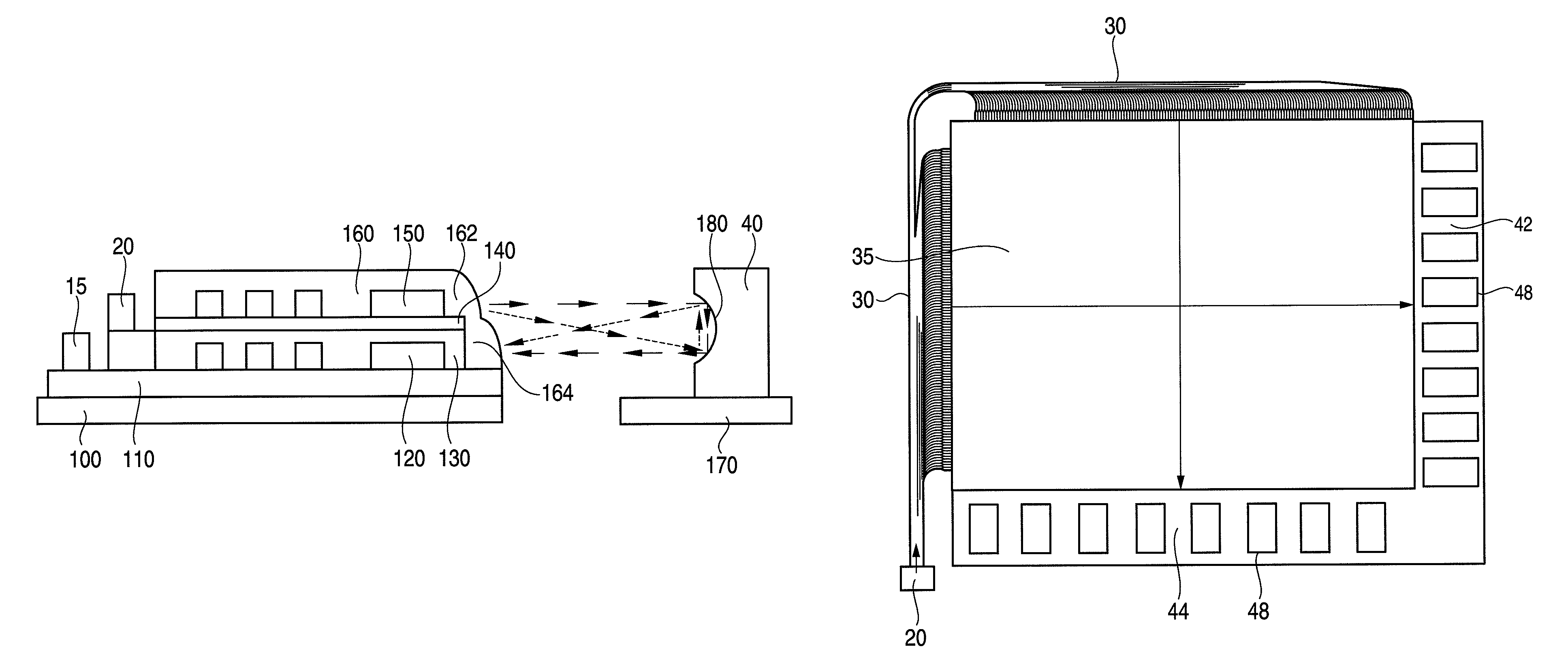
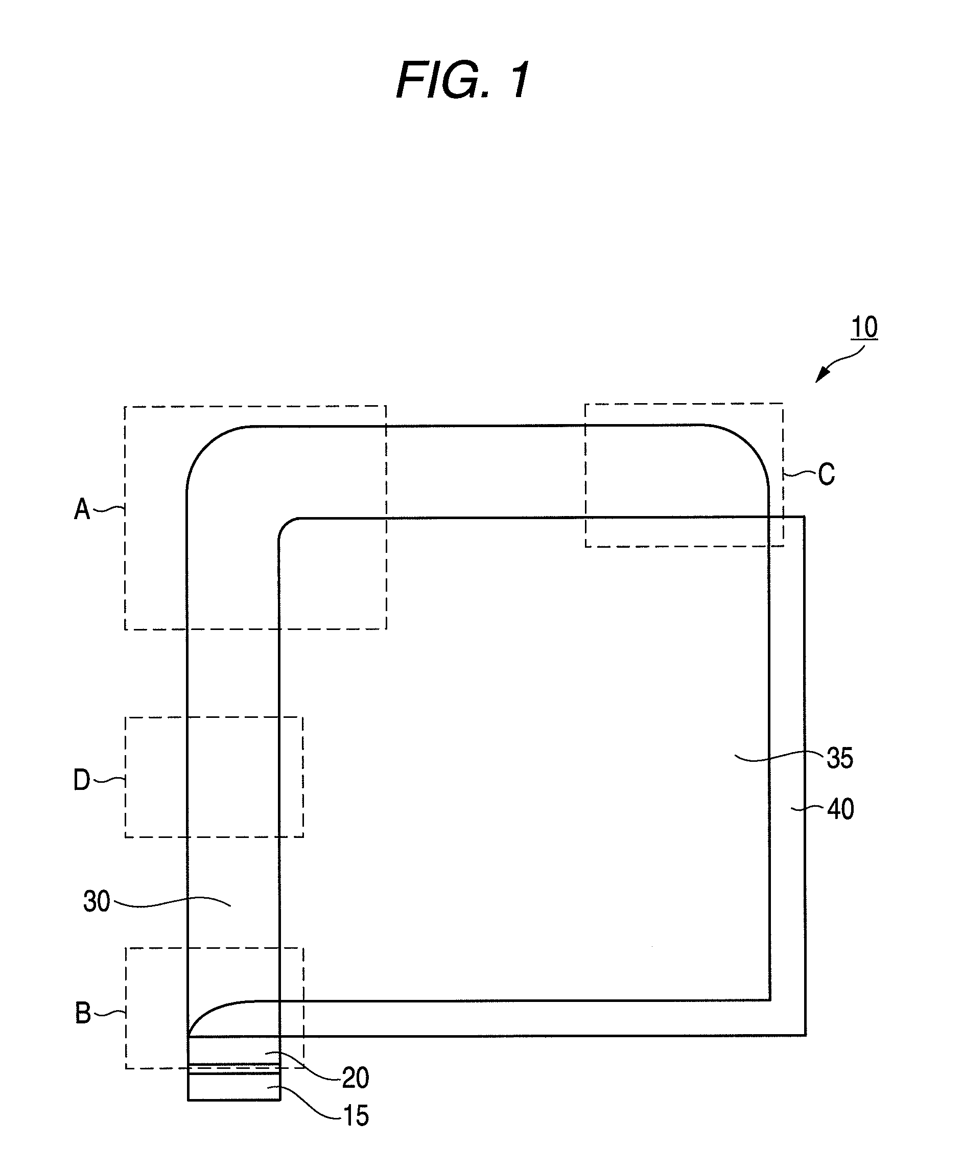
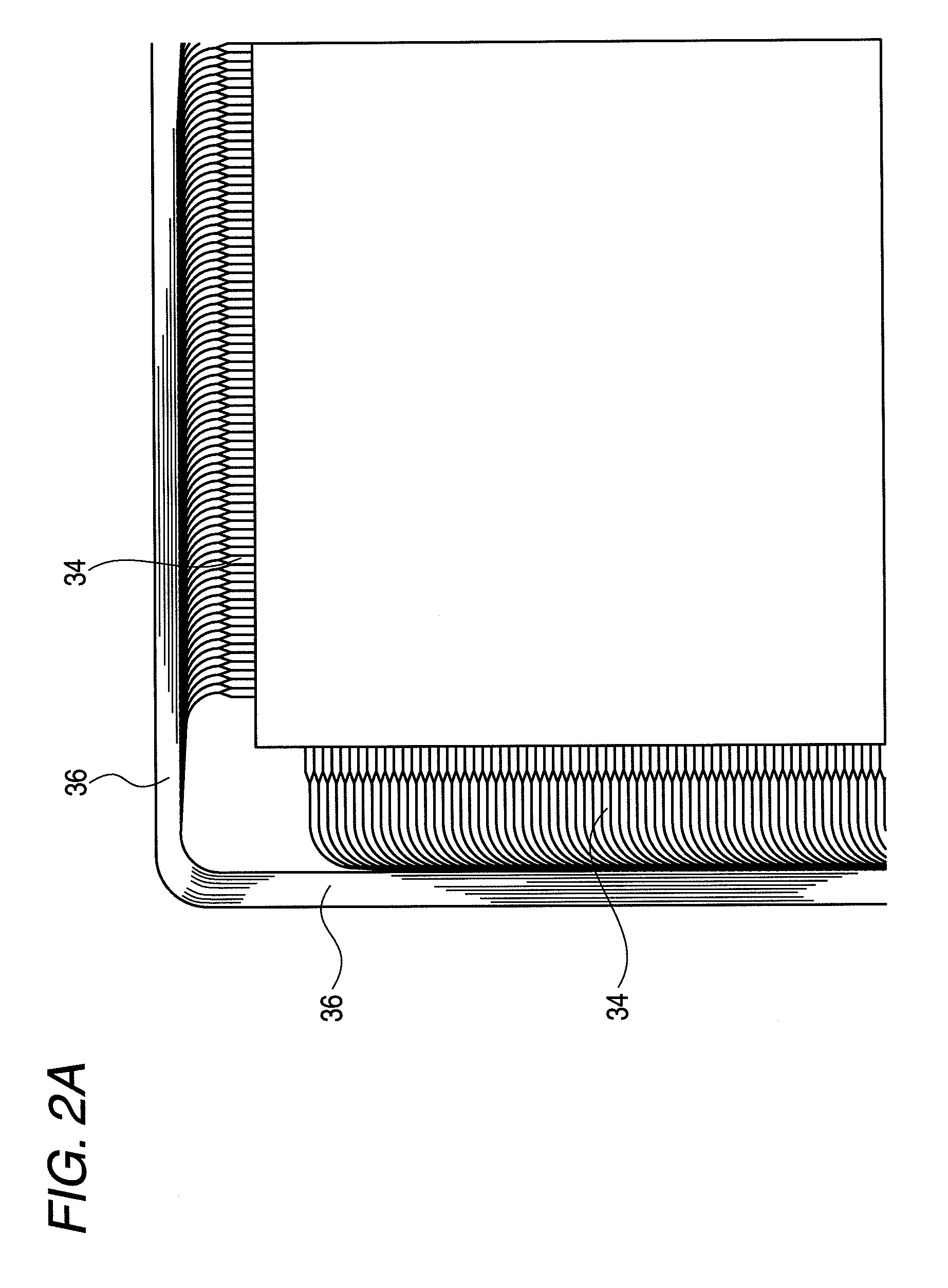
[0028]Turning now to FIG. 1, a top view of an apparatus is shown. The apparatus 10 comprises a waveguide 30, a reflector 40, a light source 20, and a light detector 15. The light source 20 is optically coupled to one end of the waveguide 30, which extends along two perpendicular sides of a detection space 35. In other words, the waveguide 30 in this exemplary embodiment extends in an “L-shape” around two perpendicular sides of the detection space 35. The reflector 40 extends along two perpendicular sides of the detection space 35 which are located opposite to the sides along which the waveguide 30 is positioned. The reflector 40 may be formed as one integral piece which extends along both of the perpendicular sides of the detection space, or the reflector 40 may be formed as two...


PUM


Abstract

An apparatus, an optical touch panel, a waveguide, and a process for producing a double layered waveguide structure are provided. The apparatus includes a waveguide having a plurality of transmission waveguide elements and a plurality of reception waveguide elements; a light source coupled to the waveguide; a light detector coupled to the waveguide; and a reflector, spaced apart from the waveguide, the reflector reflecting light emitted from the plurality of transmission waveguide elements towards the reception waveguide elements. The waveguide includes a substrate, a first cladding layer, a reception waveguide, a second cladding layer, a transmission waveguide, and a third cladding layer. The optical touch panel includes a waveguide section comprising a waveguide; a mirror; a surface emitting laser; and a detector.

Description

BACKGROUND OF THE INVENTION[0001]1. Field of the Invention[0002]Apparatuses, devices, and methods consistent with the present invention relate to apparatuses using waveguides, and, more specifically, to optical touch panels using waveguides.[0003]2. Description of the Related Art[0004]Recently, there has been growing interest among researchers and consumers in alternative input methods for industrial electronic monitors, televisions (TVs), computers, cellular phones, personal data assistants (PDAs), automated teller machines (ATMs), and many other electronic devices. Input methods such as keyboard, keypad, and mouse become less viable as electronic devices become smaller because of the relatively large amount of space required to implement a keyboard or to manipulate a mouse. Moreover, the keyboard, keypad, and mouse are mechanical devices that tend to break down when placed in harsh industrial environments.[0005]As an alternative to the above-described input methods, touch screens ...

Claims


Application Information

Patent Timeline
Patent Type & Authority Patents(United States)
IPC IPC(8): G02B6/12G02B6/10G02B6/42G06F3/042
CPCG02B6/1221G02B6/1228G02B6/125G06F3/0421G06F3/0304
Inventor KHAN, SAZZADUR RAHMANJUNI, NORIYUKITHAVEEPRUNGSRIPORN, VISIT
Owner NITTO DENKO CORP
Learn More