

3D memory array arranged for FN tunneling program and erase
a memory array and tunneling program technology, applied in the field of high density memory devices, can solve the problems of limiting the number of control gates that can be layered in this way, high manufacturing cost, and limiting the use of technology, so as to suppress the disturbance of charge stored
- Summary
- Abstract
- Description
- Claims
- Application Information
AI Technical Summary
Benefits of technology
Problems solved by technology
Method used
Image

Examples
Embodiment Construction
[0035]A detailed description of embodiments of the present invention is provided with reference to the FIGS. 1-26.
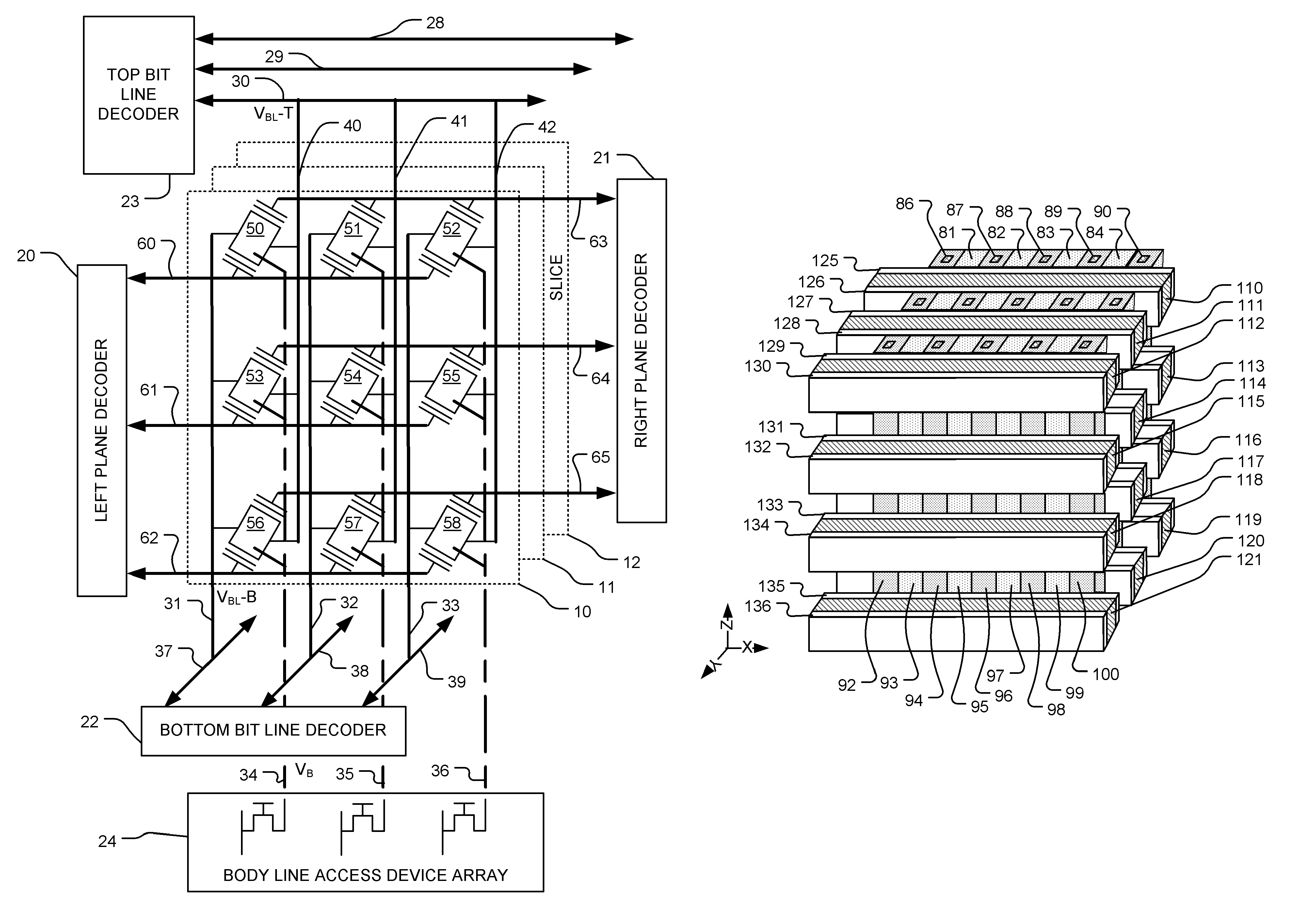
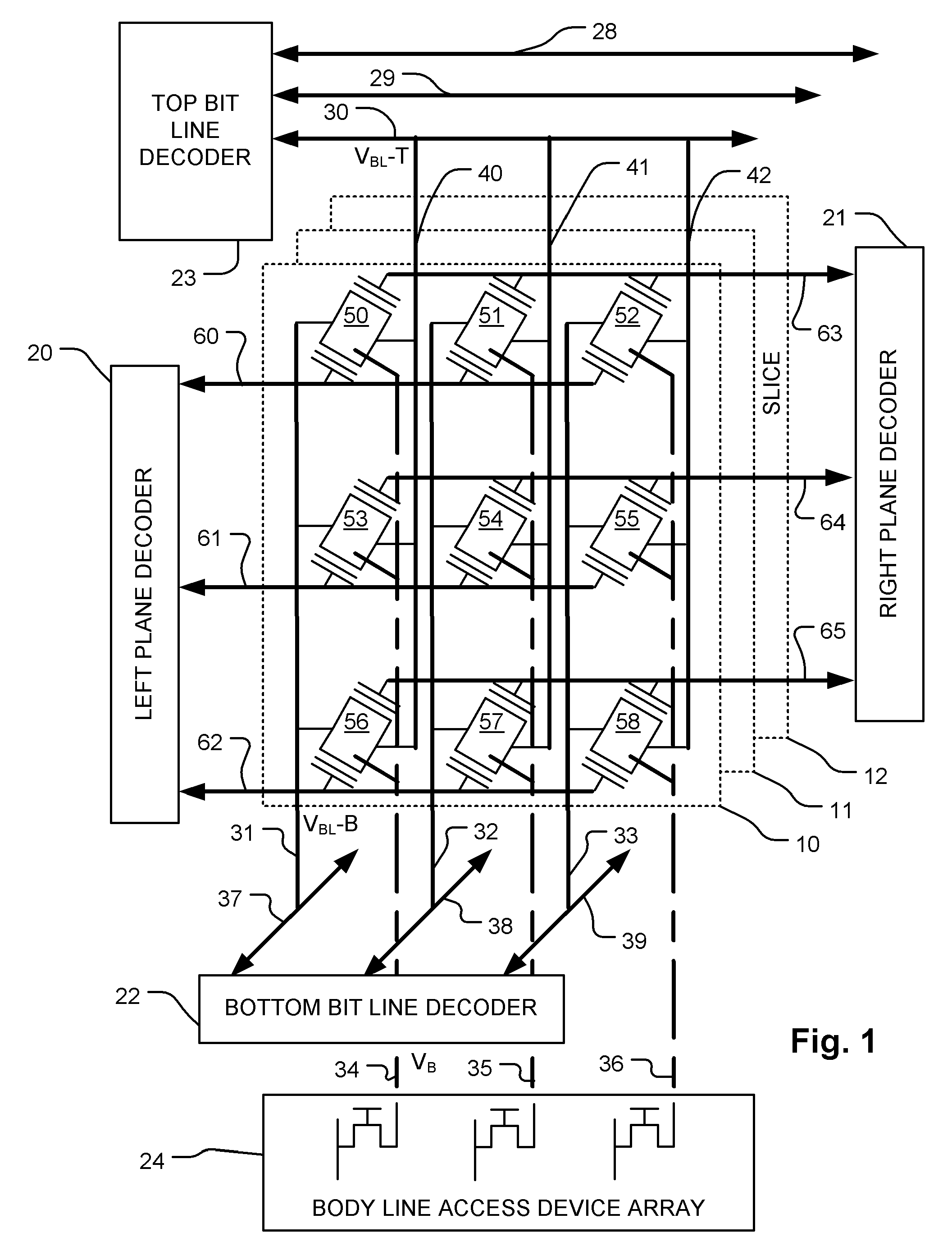
[0036]FIG. 1 is a schematic diagram of a 3D memory device, showing “slices”10, 11, 12 which lie in X-Z planes of the 3D structure. In the illustrated schematic, there are nine two-cell unit structures 50-58, each unit structure having two memory cells having separate charge storage structures and left and right gates. Embodiments of the 3D memory device can include many two-cell unit structures per slice. The device includes an array of cells arranged for AND-type decoding, using a left plane decoder 20, right plane decoder 21, top bit line (row) decoder 23, bottom bit line (column) decoder 22 and body line access device array 24. The semiconductor bodies of the two-cell unit structures in a Z-direction column (e.g. 50, 53, 56) are coupled via a semiconductor body pillar (e.g. 34) to an access device in a body line access device array 24, implemented in the integrated ci...
PUM
 Abstract
Description
Claims
Application Information