Driving circuit

a driving circuit and circuit technology, applied in the field of driving circuits, can solve the problems of insufficient guarantee of the writing period to the pixels within the panels, the resistance (wiring resistance) of the lines, and the long charging time period of the gradation voltage with respect to the hold capacity of the pixel, so as to avoid the increase in the size of the chip structure of the driving circuit and shorten the writing period to the pixel

Active Publication Date: 2012-06-19
LAPIS SEMICON CO LTD
View PDF29 Cites 0 Cited by
  • Summary
  • Abstract
  • Description
  • Claims
  • Application Information

AI Technical Summary

Benefits of technology

[0012]In accordance with the driving circuit of the present aspect, in the first time period, the second line between the second node and the output terminal is connected in parallel to the first line between the first node and the output terminal. Therefore, the parasitic resistance between the target gradation potential (first node) and the output terminal decreases, as compared with the case of only the first line. In this way, the time constant of the circuit between the target gradation potential and the output terminal is shortened.
[0014]In accordance with the present invention, the writing period to a pixel is shortened as compared with conventional structures. Further, as compared with conventional structures, there are no additional structural elements, and an increase in the size of the chip structuring the driving circuit can be avoided.

Problems solved by technology

Because the number of lines within the driving circuit thereby increases, the resistance (wiring resistance) parasitic on the lines increases, and the charging time period of the gradation voltage with respect to the hold capacity within the pixel becomes long.
Accordingly, due to the size of liquid crystal panels increasing in recent years, the writing period to the pixels within the panels has not been able to be sufficiently ensured.
On the other hand, increasing the size of the chip for forming the driving circuit in order to reduce the wiring resistance is not preferable from the standpoint of costs.

Method used


Image

  • Driving circuit
  • Driving circuit
  • Driving circuit

Examples


first exemplary embodiment

(Overall Structure of Liquid Crystal Display Device)

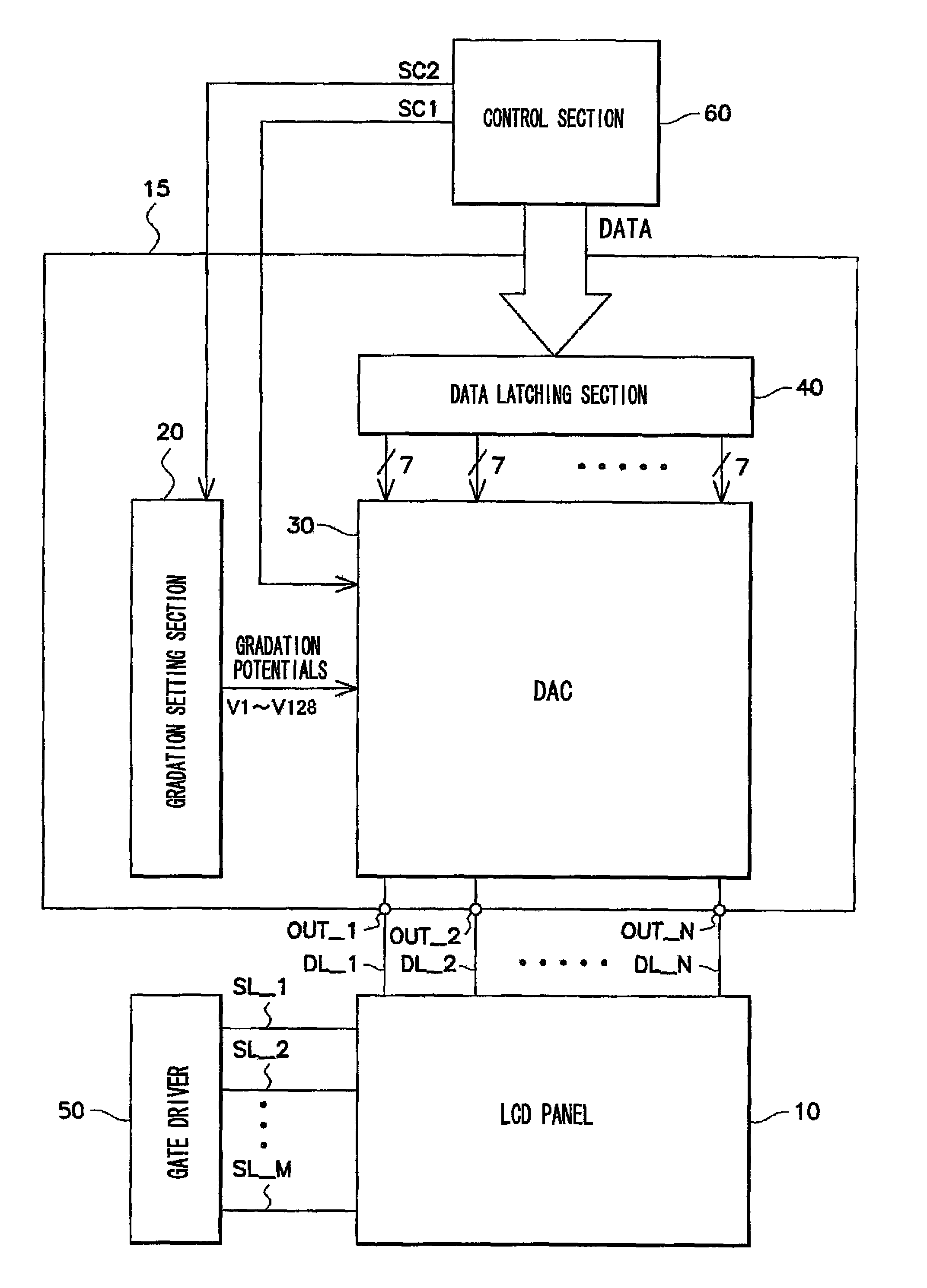
[0024]First, the overall structure of a liquid crystal display device, to which a driving circuit relating to an exemplary embodiment of the present invention is applied, will be described with reference to FIG. 1. FIG. 1 is a block diagram showing the structure of the liquid crystal display device.

[0025]Note that, in the present exemplary embodiment, explanation is given by using as an example a liquid crystal display device which processes display data of 128 gradations (7 bits). However, the present exemplary embodiment can easily be expanded to display data of different numbers of gradations (data other than 7 bits).

[0026]As shown in FIG. 1, the liquid crystal display device has a liquid crystal display panel (LCD panel) 10, a source driver 15, a gate driver 50, and a control section 60. Note that the source driver 15 and the control section 60 structure the exemplary embodiment of the driving circuit of the present invention.

[...

second exemplary embodiment

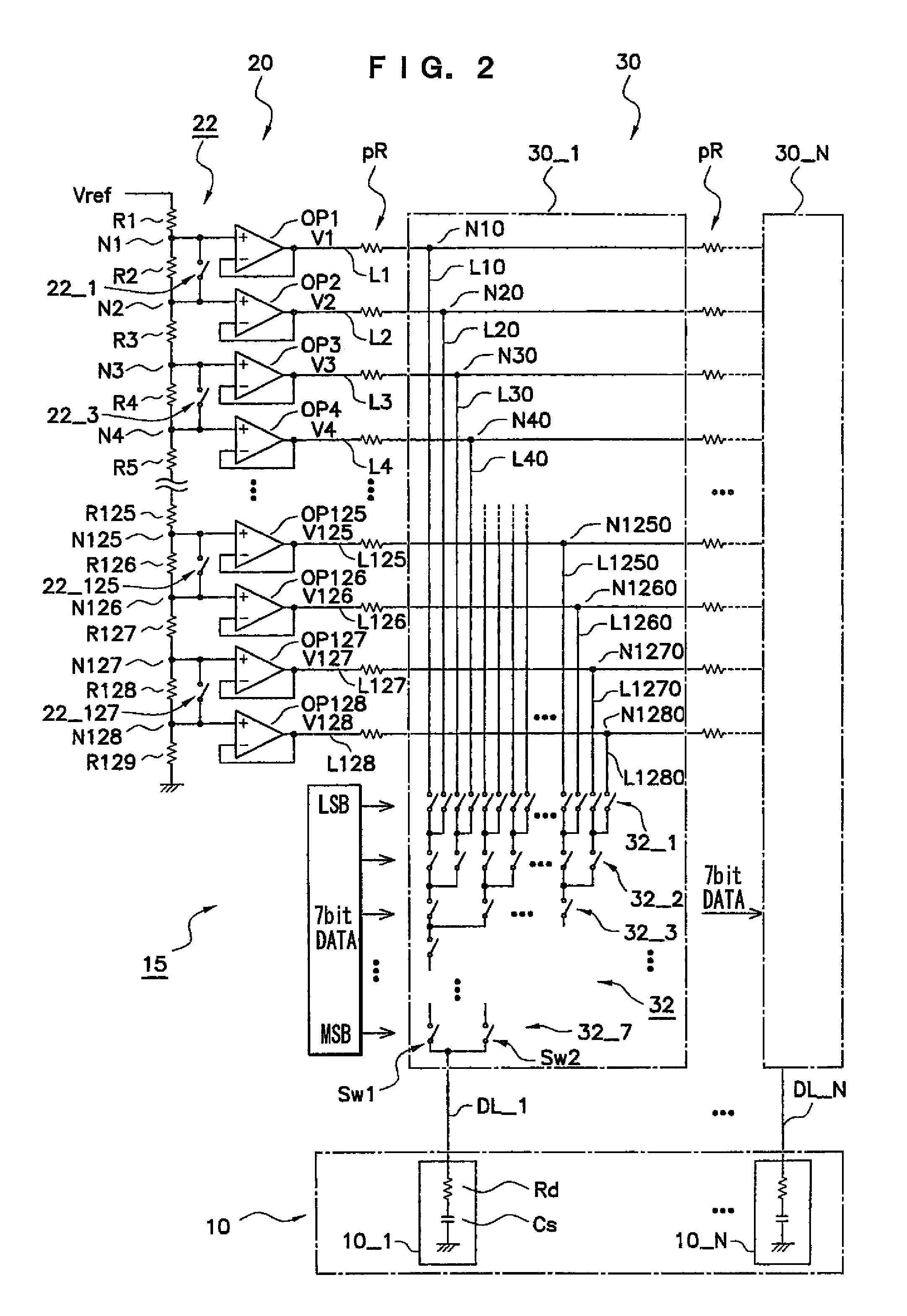
[0086]A second exemplary embodiment of a driving circuit of the present invention will be described next. In the driving circuit relating to the present exemplary embodiment, the structure of the switching element group in the gradation setting section of the source driver, and the contents of the control of the control section, are different than in the first exemplary embodiment.

[0087]FIG. 6 is a circuit diagram showing the structure of a source driver in the present exemplary embodiment. Regions which are the same as those shown in FIG. 2 are denoted by the same reference numerals, and repeat description thereof is not carried out.

(Structure of Source Driver)

[0088]A specific example of the circuit structure of a source driver 17 in the present exemplary embodiment will be described next with reference to FIG. 6.

[0089]Differently than the previously-described source driver 15 (see FIG. 2), the source driver 17 has a gradation setting section 22 which includes a switching element g...


PUM


Abstract

A driving circuit of a display device is provided. In a first time period of a data writing period, a control section of the driving circuit effects control so as to short-circuit a first node which is set to a target gradation potential and a node (second node) adjacent to the first node, and such that a line (second line) between the second node and a hold capacitor of a pixel is connected in parallel to a line (first line) between the first node and the hold capacitor of the pixel. Further, in a second time period following the first time period, the control section controls switching element groups so as to cancel short-circuiting between the first node and the second node, and such that the second line is not connected in parallel to the first line.

Description

CROSS-REFERENCE TO RELATED APPLICATION[0001]This application claims priority under 35 USC 119 from Japanese Patent Application No. 2006-197709, the disclosure of which is incorporated by reference herein.BACKGROUND OF THE INVENTION[0002]1. Field of the Invention[0003]The present invention relates to a driving circuit which drives data lines in a display device for multigradation display of pixels.[0004]2. Description of the Related Art[0005]In active matrix liquid crystal display devices, which are the mainstream of liquid crystal display devices, pixels are selectively driven in units of pixels (dot sequential driving) or in units of rows (line sequential driving).[0006]In an active matrix liquid crystal display device, pixels containing liquid crystal cells are arranged in the form of a matrix. Each pixel includes a thin film transistor (TFT), and a hold (retentive) capacitor which is connected in parallel to the liquid crystal cell. The hold capacitor is provided between the drai...

Claims


Application Information

Patent Timeline
Patent Type & Authority Patents(United States)
IPC IPC(8): G09G3/36G09G5/00G06F3/038
CPCG09G3/2011G09G3/3688G09G2320/0252G09G2310/027G09G2310/0251G09G3/36G02F1/133G09G3/20H03M1/66
Inventor NAGATOMO, SHIGERUNAKAYAMA, AKIRASUSHIHARA, AKIHIRO
Owner LAPIS SEMICON CO LTD
Why Eureka
Try Eureka