System and method for LED packaging

a technology of led packaging and reflectors, which is applied in the direction of semiconductor devices, semiconductor/solid-state device details, electrical devices, etc., can solve the problems of wasting energy and wasting conventional edison light bulbs, and achieve the effects of improving the thermal conductivity of led packages, improving efficiency, and being easy to manufactur

Active Publication Date: 2012-06-26
KORRUS INC
View PDF29 Cites 42 Cited by
  • Summary
  • Abstract
  • Description
  • Claims
  • Application Information

AI Technical Summary

Benefits of technology

[0011]The device and method of manufacture provide for improved lighting with improved efficiency. They are easier to manufacture using conventional technologies. In certain embodiments, thermal management structures are able to greatly improve thermal conductivity of the LED package. In a specific instance, thermally conductive material as a part of the conductive layer can improve thermal conductivity by almost 50%. For example, the thermal conductivity of a conventional LED package is about 13° C. / W. By increasing the thickness of conductive layers according to an embodiment of the present invention (e.g., 50 microns of copper material illustrated in FIG. 11), the thermal spreading resistance is lowered to 7° C. / W. The use of insulating layers between the reflective layer and the conductive layer greatly improves reflectivity, which translates to more usable light coming out of the LED package. These and other benefits are further described throughout the present specification and more particularly below.

Problems solved by technology

Unfortunately, the conventional Edison light bulb dissipates much thermal energy.
Additionally, the conventional light bulb eventually fails due to evaporation of the tungsten filament.
Numerous types of conventional LED packages have been used, however, they suffer from various disadvantages.

Method used


Image

  • System and method for LED packaging
  • System and method for LED packaging
  • System and method for LED packaging

Examples


Embodiment Construction

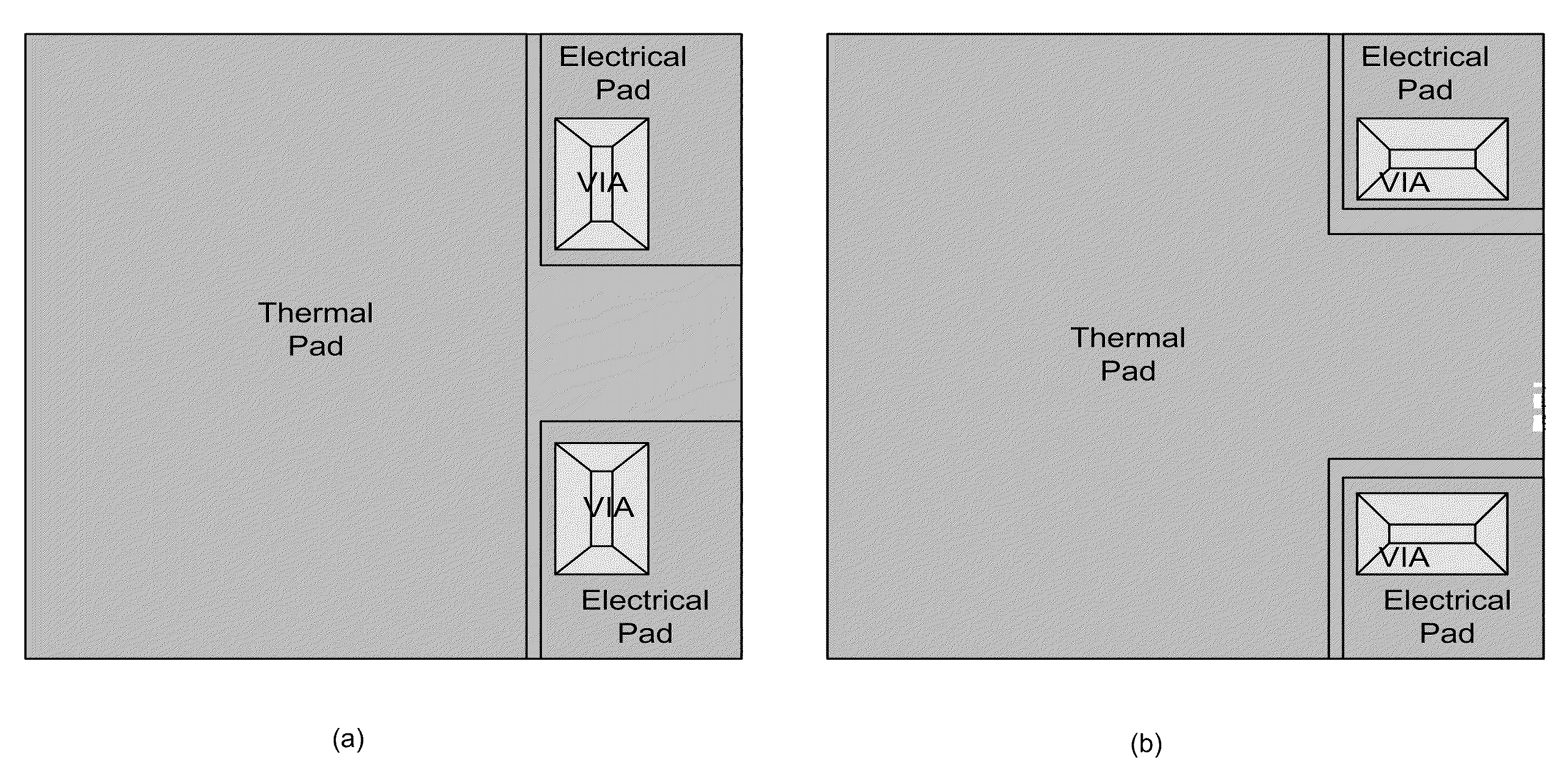
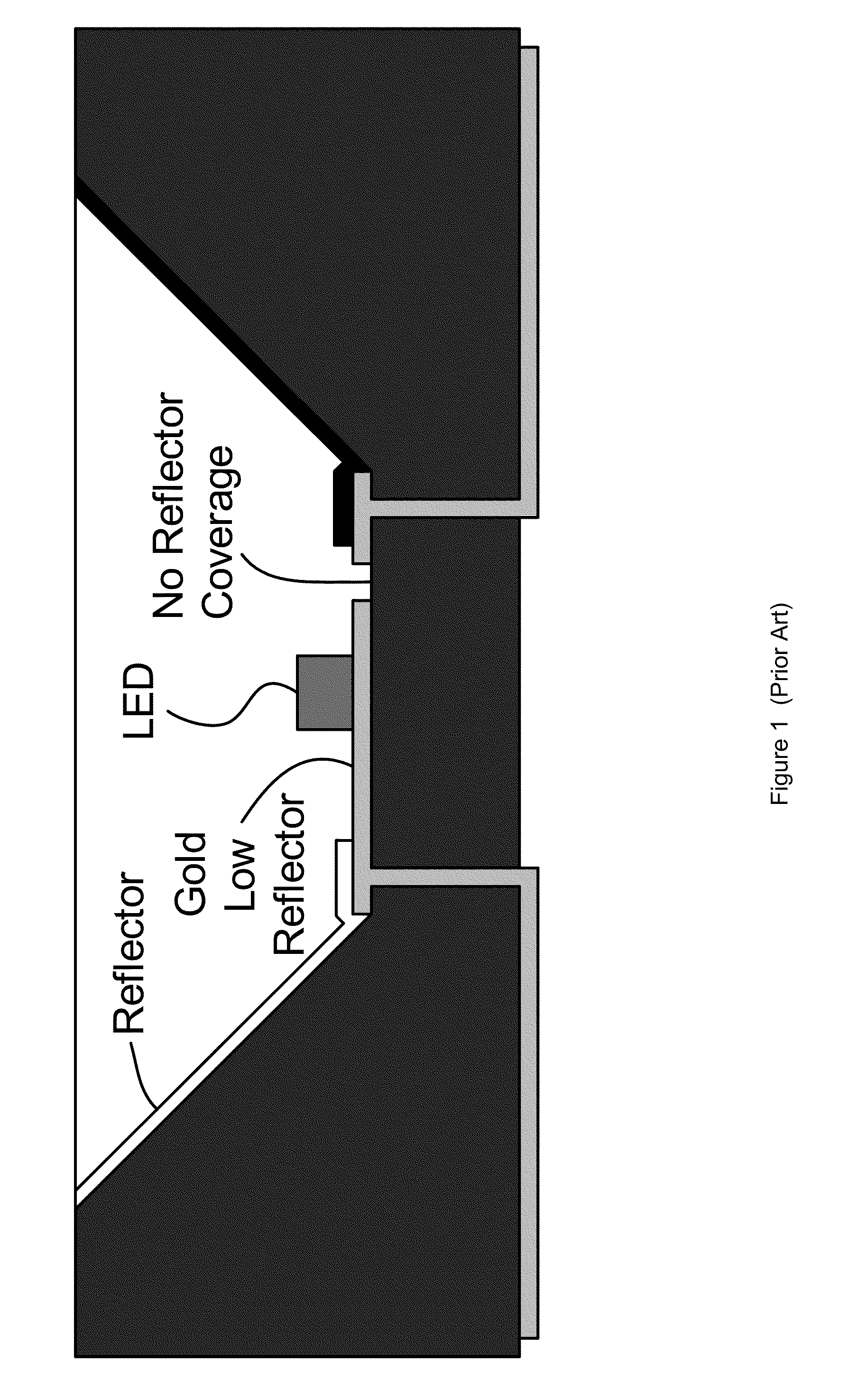
[0026]As explained above, LED chips are often used as a light source. For LED chips to function, they are secured into a package and electrically coupled to an energy source. The optical efficiency of an LED package is related the reflectivity of the cavity surfaces. FIG. 1 is a simplified diagram illustrating a conventional LED package silicon cavity. In the silicon cavity package illustrated in FIG. 1, certain regions (such as the isolation areas between electrical contacts, portion of exposed gold) have low optical reflectivity. As a result, these areas lower the overall reflectivity of the cavity and thus, the optical efficiency of the package. In addition, conventional reflectors are often inadequate.

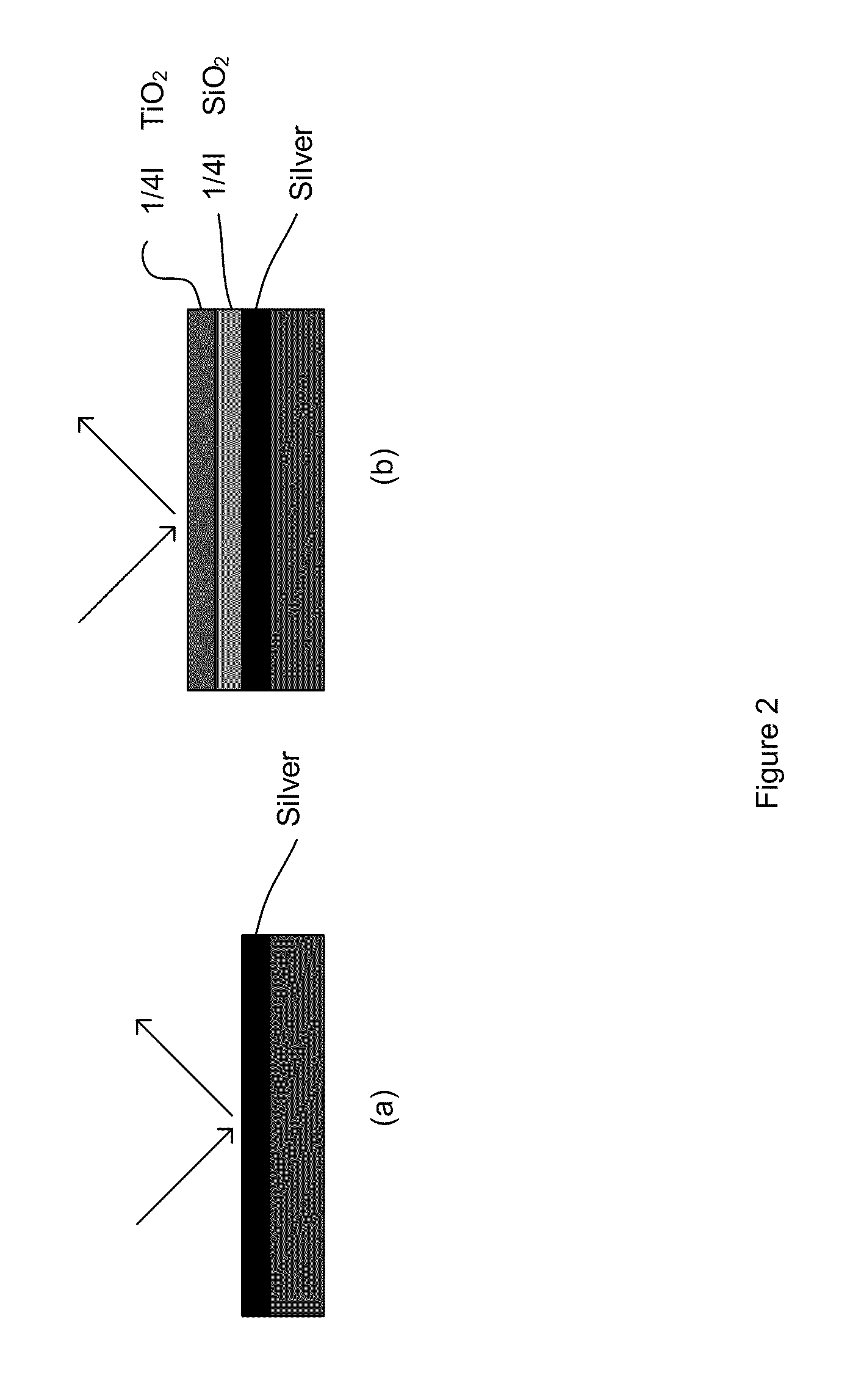
[0027]According to an embodiment, the invention provides an improved reflector. FIGS. 2(a) and 2(b) are simplified diagrams illustrating an enhancement reflector according to embodiments of the present invention. These diagrams are merely an example, which should not unduly limit t...


PUM


Abstract

System and method for LED packaging. The present invention is directed to optical devices. More specifically, embodiments of the presentation provide LED packaging having one or more reflector surfaces. In certain embodiments, the present invention provides LED packages that include thermal pad structures for dissipating heat generated by LED devices. In particular, thermal pad structures with large surface areas are used to allow heat to transfer. In certain embodiments, thick thermally conductive material is used to improve overall thermal conductivity of an LED package, thereby allowing heat generated by LED devices to dissipate quickly. Depending on the application, thermal pad structure, thick thermal conductive layer, and reflective surface may be individually adapted in LED packages or used in combinations. There are other embodiments as well.

Description

CROSS-REFERENCE TO RELATED APPLICATIONS[0001]This application claims priority from U.S. Provisional Patent Application No. 61 / 241,459, filed Sep. 11, 2009; U.S. Provisional Patent Application No. 61 / 241,457, filed Sep. 11, 2009; and U.S. Provisional Patent Application No. 61 / 241,455, filed Sep. 11, 2009, commonly assigned and incorporated by reference herein for all purposes.BACKGROUND OF THE INVENTION[0002]This invention is directed to optical devices. More specifically, embodiments of the invention provide LED packaging having reflector surfaces, and in some implementations provide LED packages that include thermal pad structures for dissipating heat generated by the LED devices. In particular, thermal pad structures with large surface areas are used to provide heat transfer. In certain embodiments, thick thermally conductive material is used to improve overall thermal conductivity of an LED package, thereby allowing heat generated by LED devices to dissipate quickly. Depending on...

Claims


Application Information

Patent Timeline
Patent Type & Authority Patents(United States)
IPC IPC(8): H01L33/00
CPCH01L33/46H01L33/60H01L33/64H01L33/486H01L2924/0002H01L2924/00
Inventor SHUM, FRANK TIN CHUNG
Owner KORRUS INC
Why Eureka
Try Eureka