Image sensor, substrate for the same, image sensing device including the image sensor, and associated methods

a technology of image sensor and image sensor, which is applied in the direction of electrical equipment, semiconductor devices, radio frequency controlled devices, etc., can solve the problems of poor device sensitivity, light reflected within the image sensor may impinge on adjacent photo diodes, and light reaching the photo diodes through the aperture, so as to reduce the amount of dark current and improve the light sensitivity

Inactive Publication Date: 2012-06-26
SAMSUNG ELECTRONICS CO LTD
View PDF15 Cites 15 Cited by
  • Summary
  • Abstract
  • Description
  • Claims
  • Application Information

AI Technical Summary

Benefits of technology

[0007]It is therefore another feature of an embodiment to provide an image sensor, a substrate for the same, an image sensing device including the image sensor, and associated methods, in which light sensitivity is improved.
[0021]The method may further include, after forming the metal interconnection structure, reducing a thickness of the first substrate by about 50% or more.
[0023]The method may further include bonding a third substrate to the first surface of the second substrate after forming the metal interconnection structure and before reducing the thickness of the first substrate by about 50% or more.

Problems solved by technology

Thus, the amount of light reaching the photo diodes through the apertures may be reduced, resulting in poor device sensitivity.
Further, light reflected within the image sensor may impinge upon adjacent photo diodes, such that cross-talk between photo diodes occurs.
However, current back side image sensor designs and manufacturing processes may suffer from drawbacks such as dark current, lack of light sensitivity, i.e., poor quantum efficiency, and the need to protect heat sensitive structures during manufacturing.

Method used


Image

  • Image sensor, substrate for the same, image sensing device including the image sensor, and associated methods
  • Image sensor, substrate for the same, image sensing device including the image sensor, and associated methods
  • Image sensor, substrate for the same, image sensing device including the image sensor, and associated methods

Examples


first embodiment

[0059]FIGS. 1 to 7 illustrate cross-sectional views of stages in a method of fabricating an image sensor according to a As described in detail below, the stages of fabrication are ordered so as to enable the use of processes having a high heat budget before the formation of heat-sensitive structures. This allows the use of materials and processes that may be more effective at minimizing interface traps and unwanted depletion regions in the resulting image sensor, thereby improving performance of the image sensor.

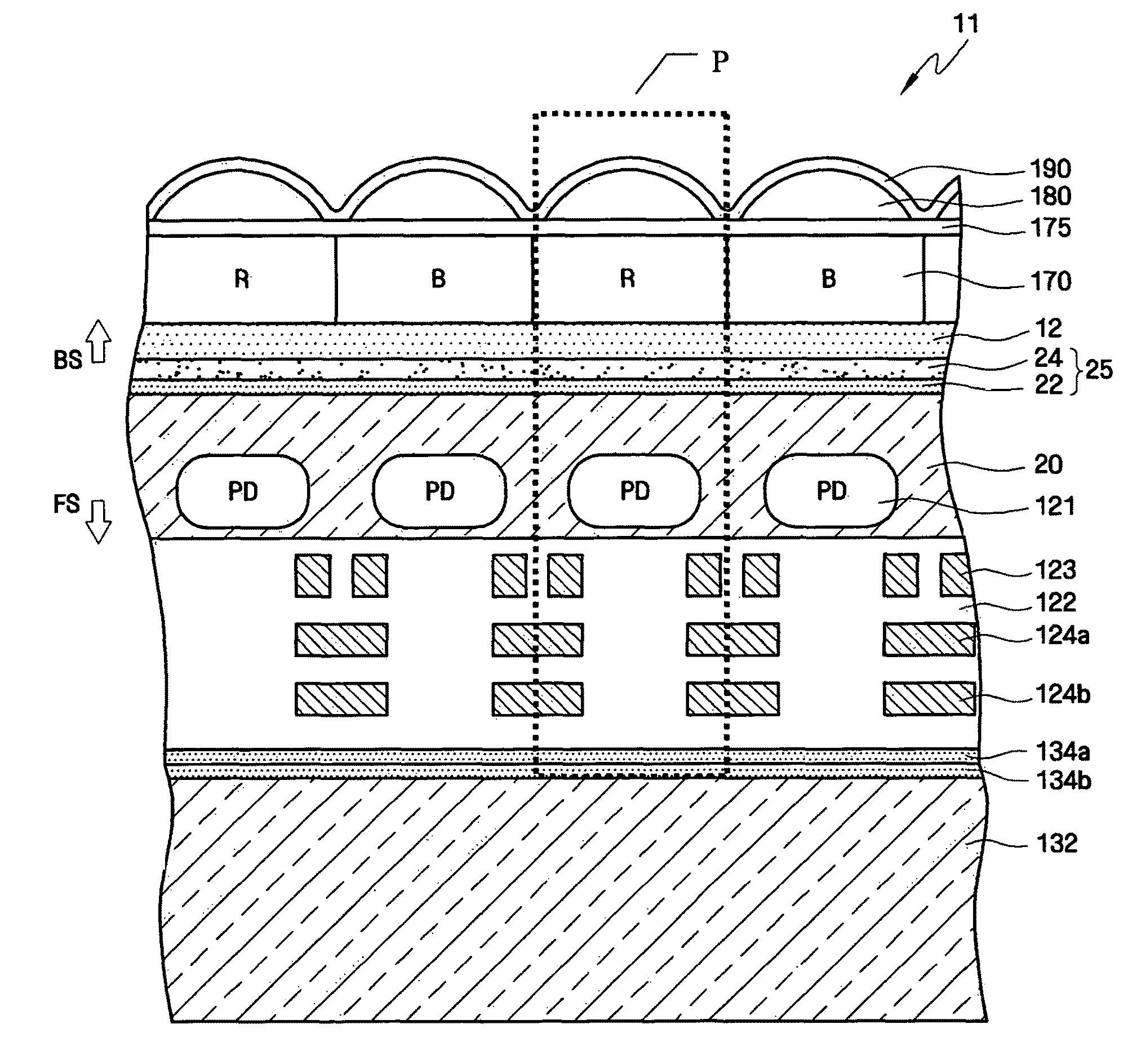
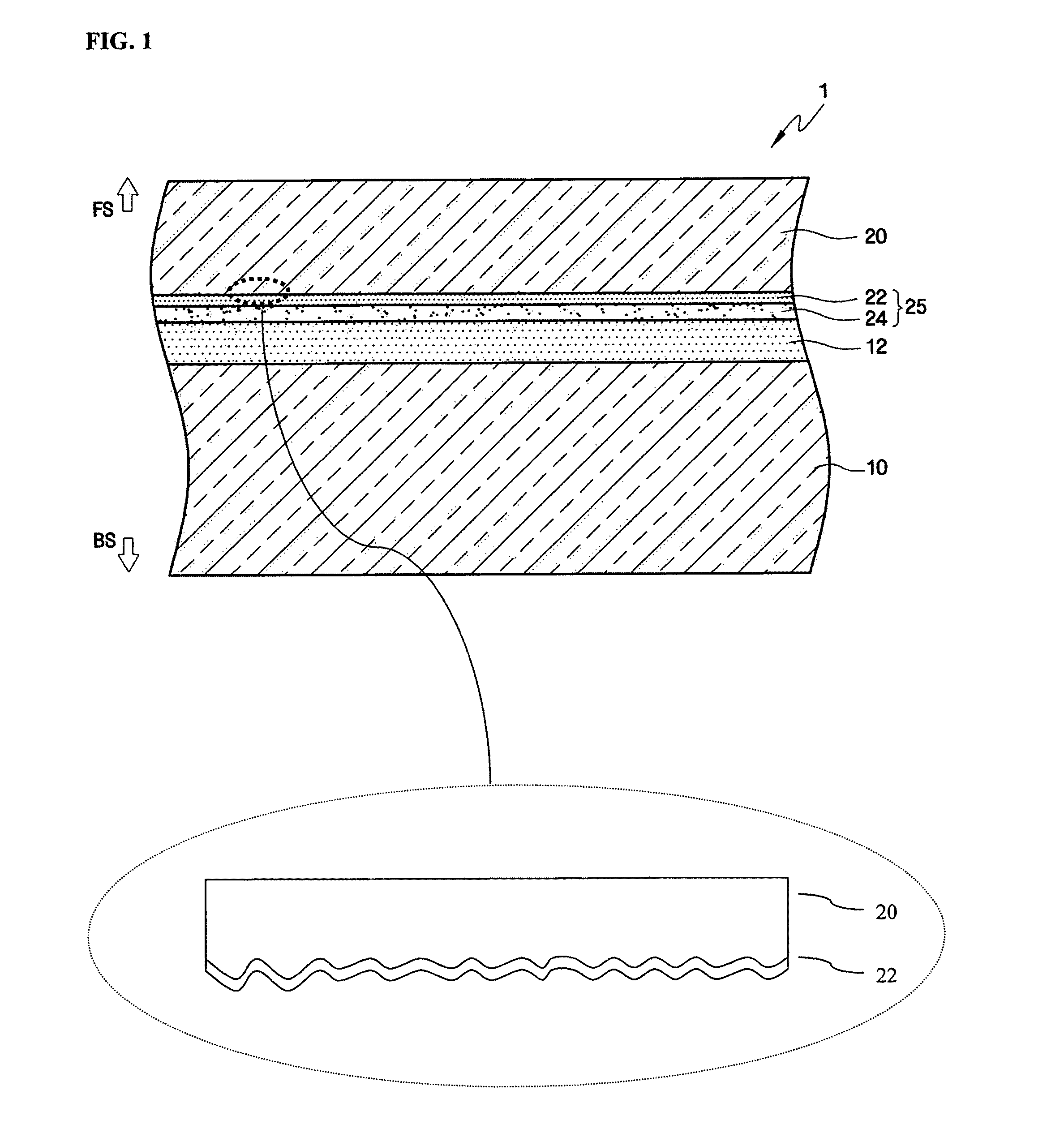
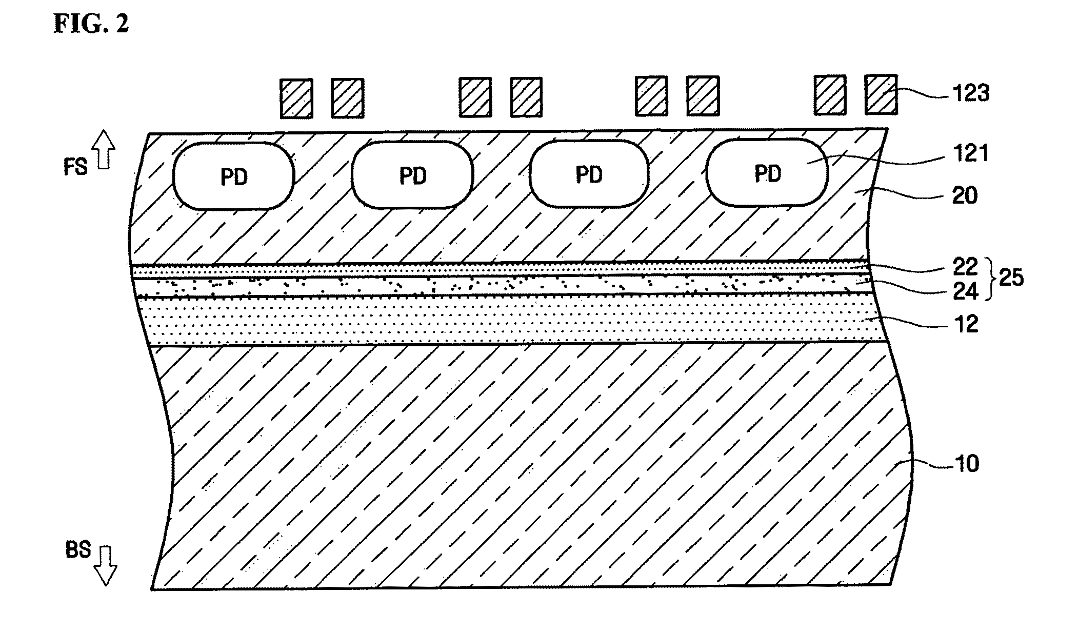
[0060]Referring to FIG. 1, a first substrate 10 and a second substrate 20 may be joined together. As described in detail below, the second substrate 20 may be processed to form a plurality of photo diodes therein, and the first substrate may be partially or completely removed so as to provide a light-sensing area proximate to the photo diodes. Thus, a backside image sensor may be provided.

[0061]Further, an oxide layer 22, preferably a thermal oxide, may be disposed between ...

second embodiment

[0081]FIG. 8A illustrates an image sensor in which one or more isolation layers ‘a’ may be formed to reduce cross-talk between adjacent light sensing devices 121. The isolation layers ‘a’ may be disposed between individual photo diodes PD, between adjacent unit pixels, etc.

[0082]Note that FIG. 8A is a composite illustration showing various implementations of the isolation layers ‘a’ in a single FIGURE. It will be appreciated that any one implementation isolation layers ‘a’ may be used alone, or in combination with one or more other implementations isolation layers ‘a’. In a first implementation, an isolation layer a1 may be formed to extend from a region adjacent to a bottom portion of a photo diode PD to the surface FS of the second substrate 20. In a second implementation, an isolation layer a2 may be formed to contact the oxide layer 22 and extend to the surface FS of the second substrate 20. In a third implementation, an isolation layer a3 may be formed to pass through the anti...

third embodiment

[0095]FIG. 9A illustrates a cross-sectional view of a stage in a method of fabricating an image sensor according to a By way of reference, FIG. 9A generally corresponds to the stage illustrated in FIG. 1. Details of features shown in FIG. 1 and common to FIG. 9A have been described above and will not be repeated. Additionally, subsequent processing stages have been described above, and will not be repeated.

[0096]Referring to FIG. 9A, a shallow implant layer 28, which serves as a pinning layer, may be formed adjacent to the second substrate 20. The shallow implant layer 28 may be disposed between the bulk of the second substrate 20 and the oxide layer 22. The shallow implant layer 28 may further reduce the concentration of interfacial traps between the second substrate 20 and the oxide layer 22, such that the dark current may be further reduced and the light sensitivity may be further enhanced.

[0097]In the case that the second substrate 20 has p-type conductivity, the shallow implan...


PUM


Abstract

A method of fabricating a CMOS image sensor includes forming a substrate structure that includes a first substrate, a second substrate, and an index matching layer containing nitrogen and an oxide layer between the first and second substrates, and, forming at least one light-sensing device in the second substrate, and after forming the substrate structure, forming a metal interconnection structure on a first surface of the second substrate, the first surface facing away from the first substrate, such that the at least one light sensing device is between the metal interconnection structure and the index matching layer and the oxide layer, the metal interconnection structure being electrically connected to the at least one light-sensing device.

Description

BACKGROUND[0001]1. Field[0002]Embodiments relate to an image sensor, a substrate for the same, an image sensing device including the image sensor, and associated methods.[0003]2. Description of the Related Art[0004]An image sensor may be formed as a “front side” CMOS image sensor that includes a plurality of photo diodes in a substrate. After forming the photo diodes, metal wiring patterns may be formed on the photo diodes. The metal wiring patterns may be formed to provide apertures for the photo diodes to receive external light. However, light entering the apertures at an angle may be reflected by the metal wiring patterns. Further, an interlayer dielectric layer surrounding the metal wiring patterns may absorb light incident thereon. Thus, the amount of light reaching the photo diodes through the apertures may be reduced, resulting in poor device sensitivity. Further, light reflected within the image sensor may impinge upon adjacent photo diodes, such that cross-talk between phot...

Claims


Application Information

Patent Timeline
Patent Type & Authority Patents(United States)
IPC IPC(8): H01L31/05
CPCH01L27/14621H01L27/14627H01L27/1464H01L27/14685H01L27/1463
Inventor PARK, BYUNG-JUNKIM, SANG-HEE
Owner SAMSUNG ELECTRONICS CO LTD
Why Eureka
Try Eureka