Method of detecting electromagnetic radiation with bandgap engineered active pixel cell design

a technology of active pixel cell and bandgap, which is applied in the direction of material analysis, radio frequency control devices, instruments, etc., can solve the problems of short wavelength radiation being easily absorbed in the pinning layer, still thick enough to absorb an undetectable high proportion, and retaining the electron in the photosensitive region. , to achieve the effect of improving blue light sensitivity and decreasing the thickness of the pinning layer

Inactive Publication Date: 2001-08-21
GLOBALFOUNDRIES INC
View PDF26 Cites 17 Cited by
  • Summary
  • Abstract
  • Description
  • Claims
  • Application Information

AI Technical Summary

Benefits of technology

The present invention comprises a method of detecting electromagnetic radiation with a photosensitive device in which blue light sensitivity is improved by dramatically decreasing the thickness of the pinning layer. This is accomplished by producing a "virtual" pinning layer through a local inversion of the surface of the photosensitive region. This inversion produces a very shallow pinning layer which can be as shallow as 0.01 micrometers in depth or less. With this extremely shallow pinning layer, blue light absorption is almost negligible.

Problems solved by technology

Electrons, however, remain trapped in the photosensitive region until a transfer device removes them.
One problem with prior art APS designs relates to the fact that short wavelength radiation is easily absorbed in the pinning layer where there are many holes available.
However, this heat causes diffusion of the implanted ions generating a pinning layer which is thicker than desired.
A pinning layer constructed in this way, while relatively shallow as compared to other layers in MOS devices, is still thick enough to absorb an undesirably high proportion of incoming short wavelength blue light.
Because the absorbed photons do not reach the underlying photosensitive region, they cannot produce the necessary hole-electron pairs in that region.
Yet another difficulty with prior art APS devices relates to the absorption of long wavelength radiation.
Thus, they easily penetrate the pinning layer.
However, for the same reason, absorption in the semiconductor material of the photosensitive region is also relatively poor.
However, each of these approaches is either expensive or is difficult to integrate into standard MOS production processes.

Method used


Image

  • Method of detecting electromagnetic radiation with bandgap engineered active pixel cell design
  • Method of detecting electromagnetic radiation with bandgap engineered active pixel cell design
  • Method of detecting electromagnetic radiation with bandgap engineered active pixel cell design

Examples


Embodiment Construction

)

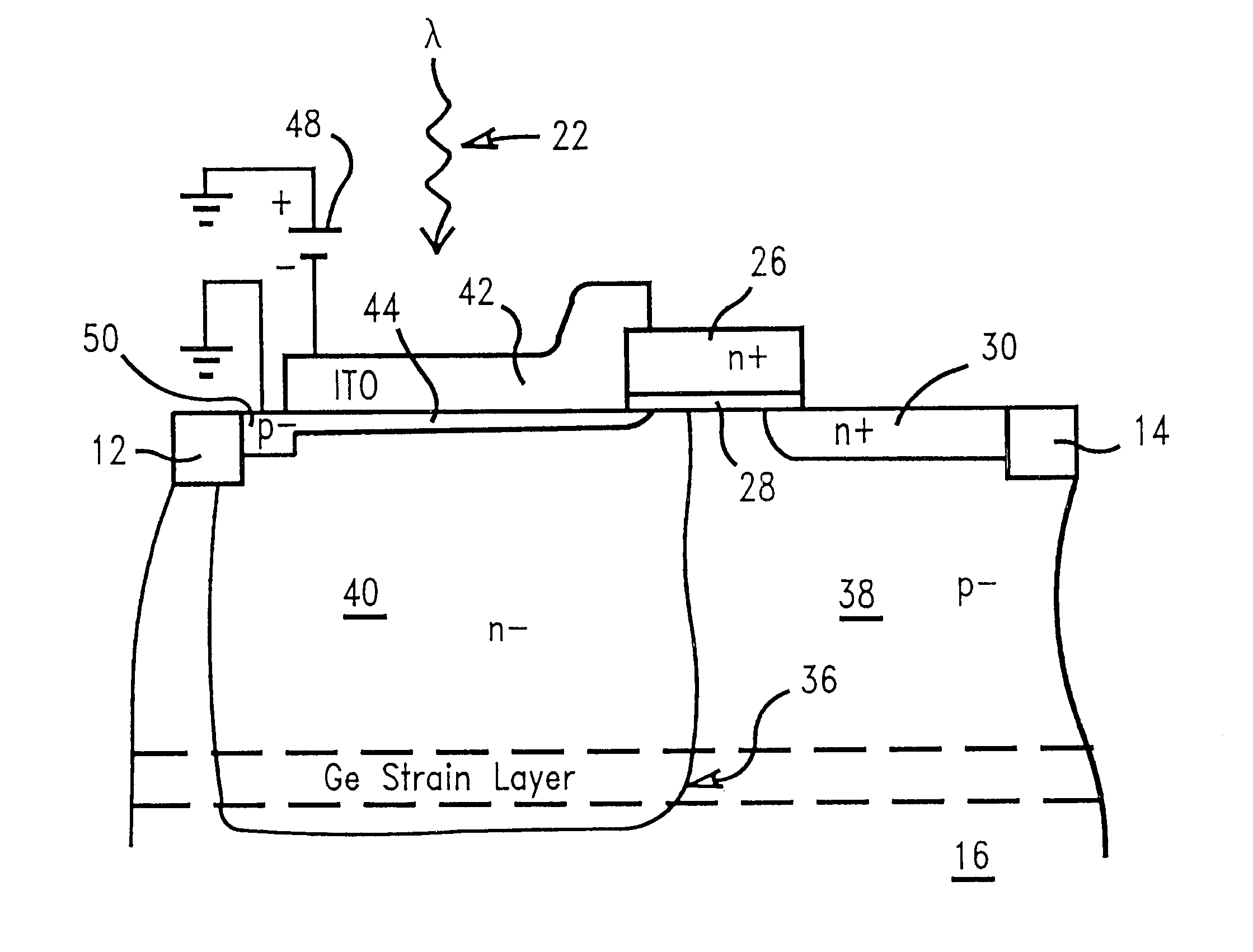
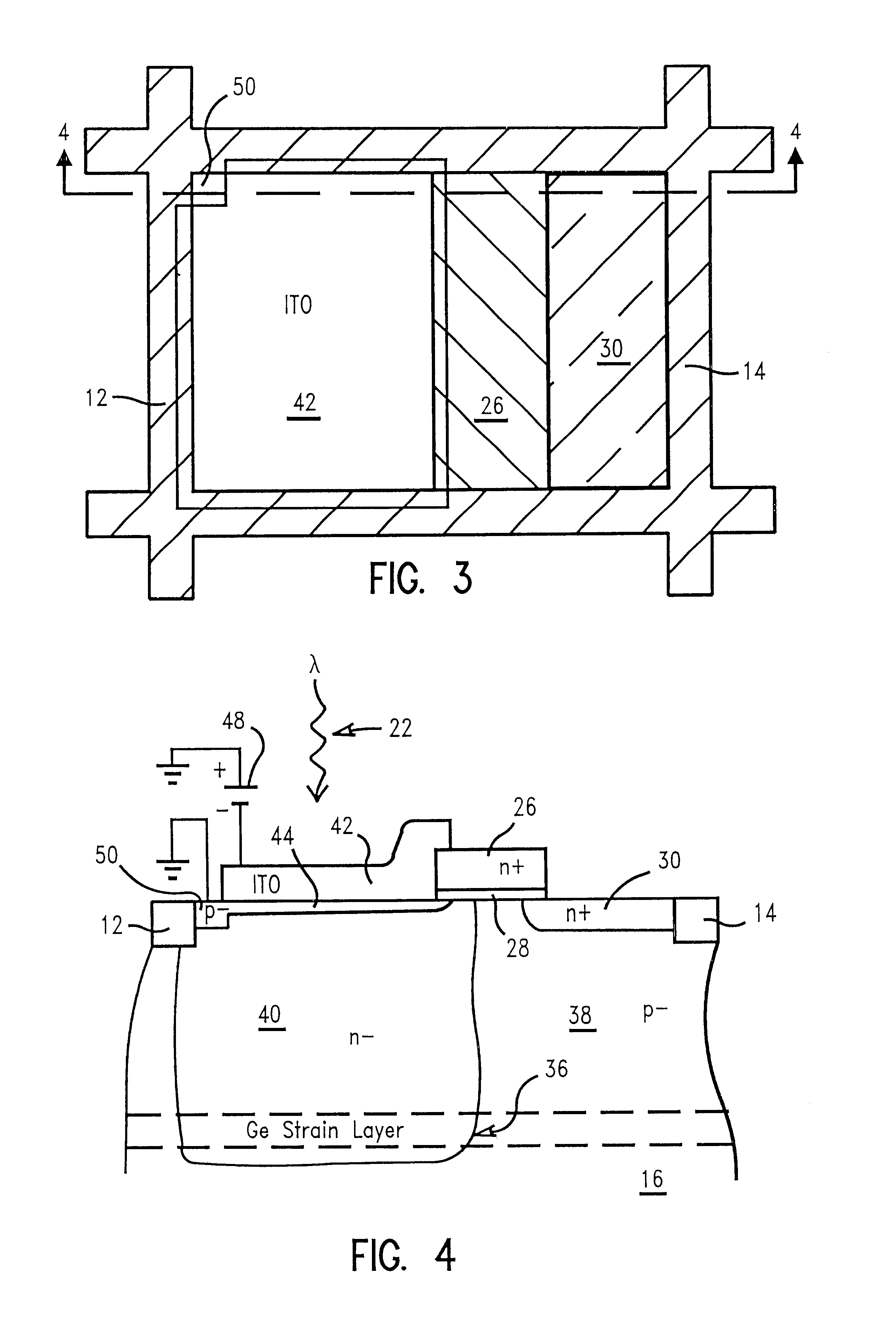
In describing the preferred embodiment of the present invention, reference will be made herein to FIGS. 1-4 of the drawings in which like numerals refer to like features of the invention.

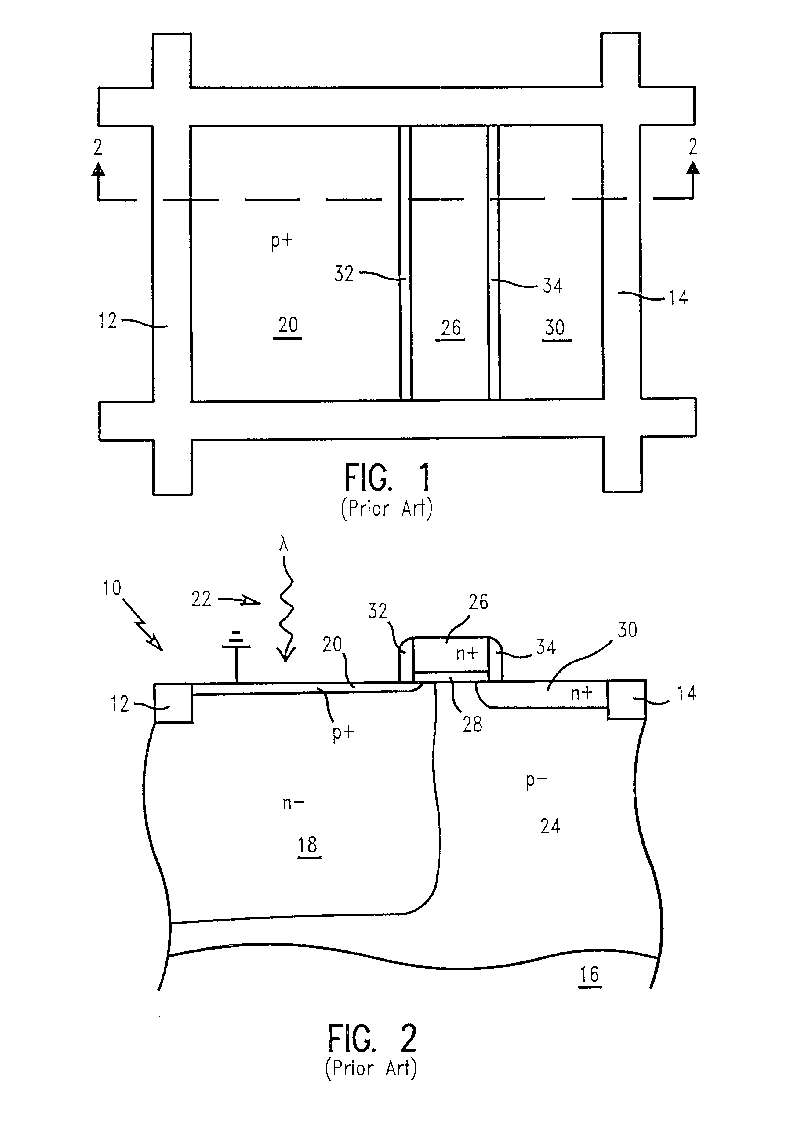
The benefits of the invention shown in FIGS. 3 and 4 will best be understood by first considering the construction of the prior art APS device shown in FIGS. 1 and 2. The prior art device shown there is generally indicated with reference numeral 10. This cell is separated from identical adjacent APS cells in an array of such cells which are located above, below and to either side, by a shallow trench isolation (STI) barrier. The left and right sides of the surrounding STI barrier are indicated with reference numerals 12 and 14 respectively.

The prior art APS device 10 is constructed on a substrate 16 and includes a relatively deep photosensitive region 18 of n- semiconductor material. A pinning layer 20 of p+ semiconductor material is grounded and is used to remove holes generated in the photosensit...


PUM

PropertyMeasurementUnit
depthaaaaaaaaaa
thicknessaaaaaaaaaa
thicknessaaaaaaaaaa

Abstract

A method of detecting electromagnetic radiation with an active pixel sensor photosensitive device having an extremely thin virtual pinning layer formed by inverting semiconductor material at the surface of a photosensitive region. The thin pinning layer improves blue light response. The inverted pinning layer is produced by connecting a negative potential source to a transparent conductive layer, preferably made of indium-tin-oxide positioned over most of the photosensitive region. The conductive layer is insulated from the photosensitive region by a thin insulating layer. Connection to the pinning layer is through a coupling region formed in an area not covered by the conductive and insulating layers. Red light response is improved and the depth of the photosensitive region reduced by creating a strained layer, preferably of germanium silicon, deep within the photosensitive region. The strained layer has a modified bandgap which increases the absorption rate of red light.

Description

1. Field of the InventionThis invention relates to solid state image sensors, and more particularly, to active pixel sensor (APS) technology.2. Description of Related ArtActive pixel sensors, like charge coupled devices (CCD) are solid state photosensitive devices. Typically, the devices are organized into an array of photosensitive cells, with each cell in the array corresponding to a pixel. A typical application for CCD or APS image sensing arrays is in a digital camera, although there are many other known applications.One advantage to APS devices over CCD devices is that APS technology is more compatible with metal oxide semiconductor (MOS) technology. This allows the support electronics needed to read signals from the APS array, and to process those signals, to be constructed on the same chip and at the same time as the APS array itself. This can significantly reduce the total cost of an APS technology based imaging device.A basic prior art APS device comprises a reversed biased...

Claims


Application Information

Patent Timeline
Patent Type & Authority Patents(United States)
IPC IPC(8): H01L27/146H01L31/10
CPCH01L27/14609H01L27/14603H01L31/101
Inventor HOOK, TERENCE B.JOHNSON, JEFFREY B.LEIDY, ROBERTWONG, HON-SUM P.
Owner GLOBALFOUNDRIES INC
Why Eureka
Try Eureka