Photo sensor and light emitting display having the same

a light emitting display and photo sensor technology, applied in the field of photo sensors, can solve the problems of inability to adjust the brightness of the light source, the brightness output of the conventional organic light emitting display may be too high, and the brightness output of the conventional organic light emitting display may be too low, so as to improve the light sensitivity to external light

Active Publication Date: 2009-02-05
SAMSUNG DISPLAY CO LTD
View PDF8 Cites 17 Cited by
  • Summary
  • Abstract
  • Description
  • Claims
  • Application Information

AI Technical Summary

Benefits of technology

[0008]It is therefore a feature of an embodiment of the present invention to provide a photo sensor with light incidence units capable of improving light sensitivity to external light.
[0009]It is another a feature of an embodiment of the present invention to provide a photo sensor for controlling brightness output of an organic light emitting display in accordance with external light.

Problems solved by technology

The conventional OLEDs, however, may have a predetermined brightness range regardless of external light, so brightness output from the conventional organic light emitting display may be unaffected by changes in external luminance.
For example, when external luminance is high, brightness output from the conventional organic light emitting display may be too low, and when external luminance is low, brightness of from the conventional organic light emitting display may be too high.
As such, contrast in the conventional organic light emitting display may be reduced, so image visibility may be deteriorated.
In addition, the predetermined brightness range of the OLEDs may increase power consumption of the conventional light emitting display.

Method used


Image

  • Photo sensor and light emitting display having the same
  • Photo sensor and light emitting display having the same
  • Photo sensor and light emitting display having the same

Examples


Embodiment Construction

[0024]Korean Patent Application No. 10-2007-0077473, filed on Aug. 1, 2007, in the Korean Intellectual Property Office, and entitled: “Photo Sensor and Light Emitting Display Having the Same,” is incorporated by reference herein in its entirety.

[0025]Embodiments of the present invention will now be described more fully hereinafter with reference to the accompanying drawings, in which exemplary embodiments of the invention are illustrated. Aspects of the invention may, however, be embodied in different forms and should not be construed as limited to the embodiments set forth herein. Rather, these embodiments are provided so that this disclosure will be thorough and complete, and will fully convey the scope of the invention to those skilled in the art.

[0026]In the figures, the dimensions of layers, elements, and regions may be exaggerated for clarity of illustration. It will also be understood that when a layer or element is referred to as being “on” another layer, element, or substra...


PUM


Abstract

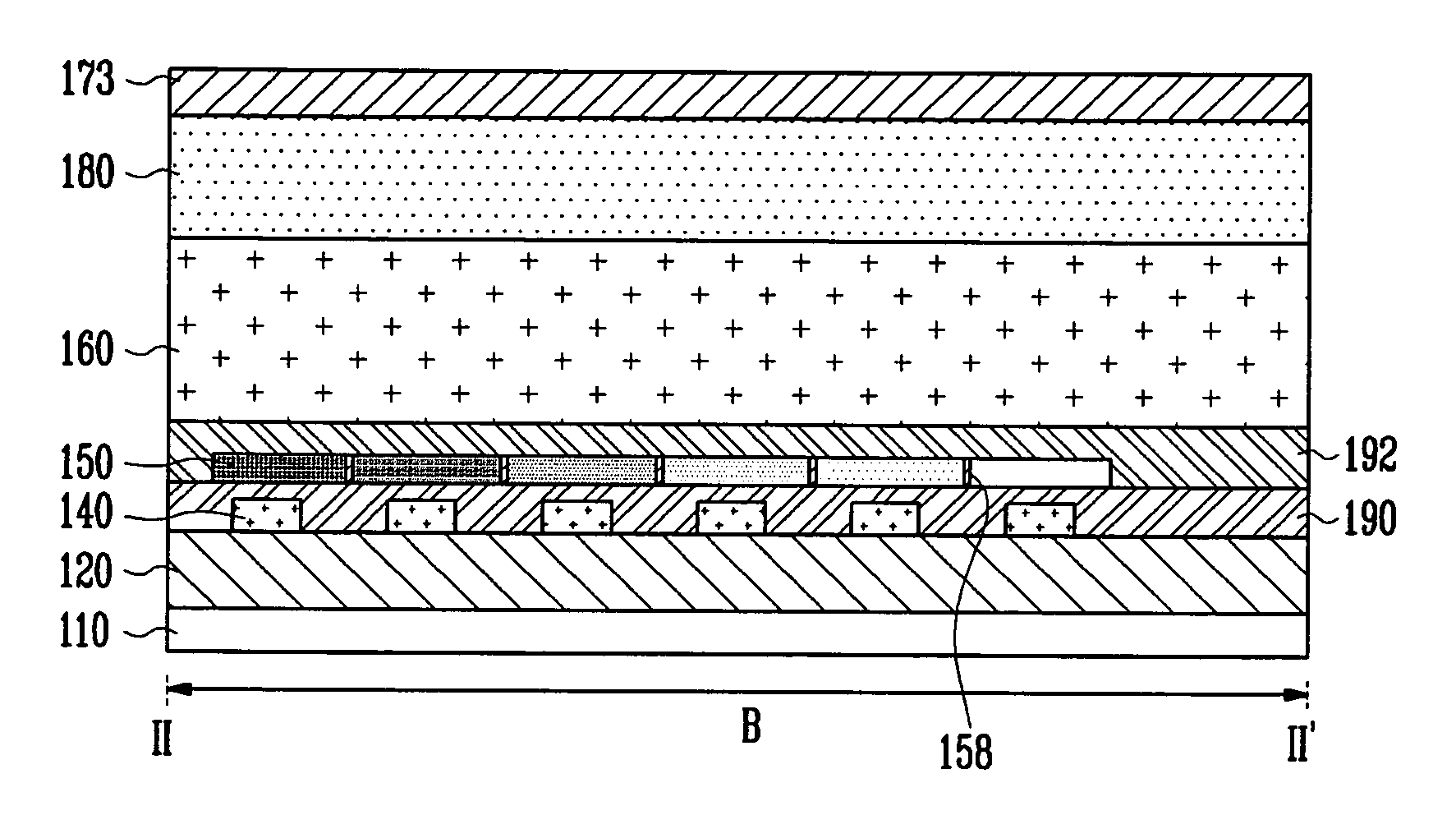
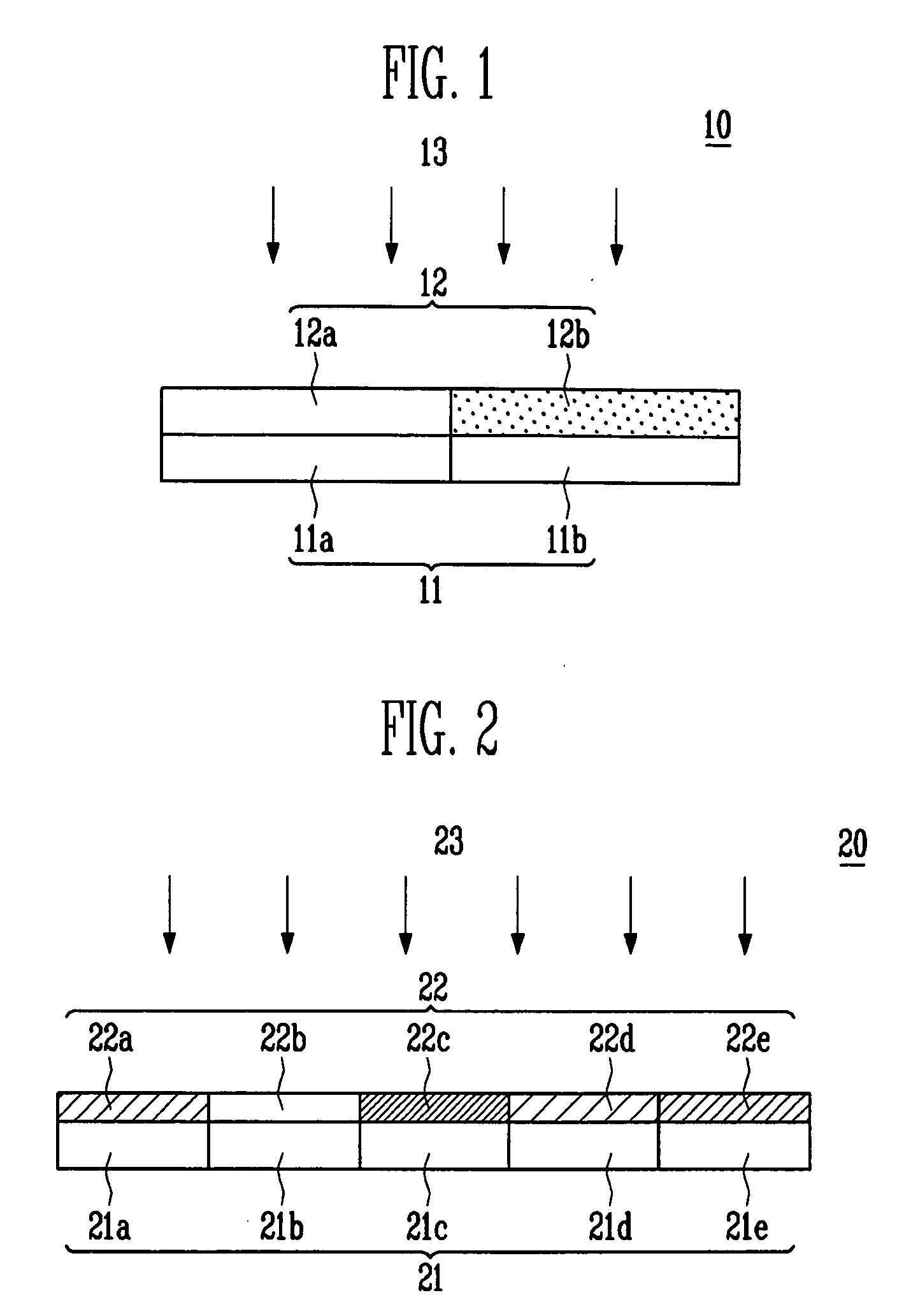
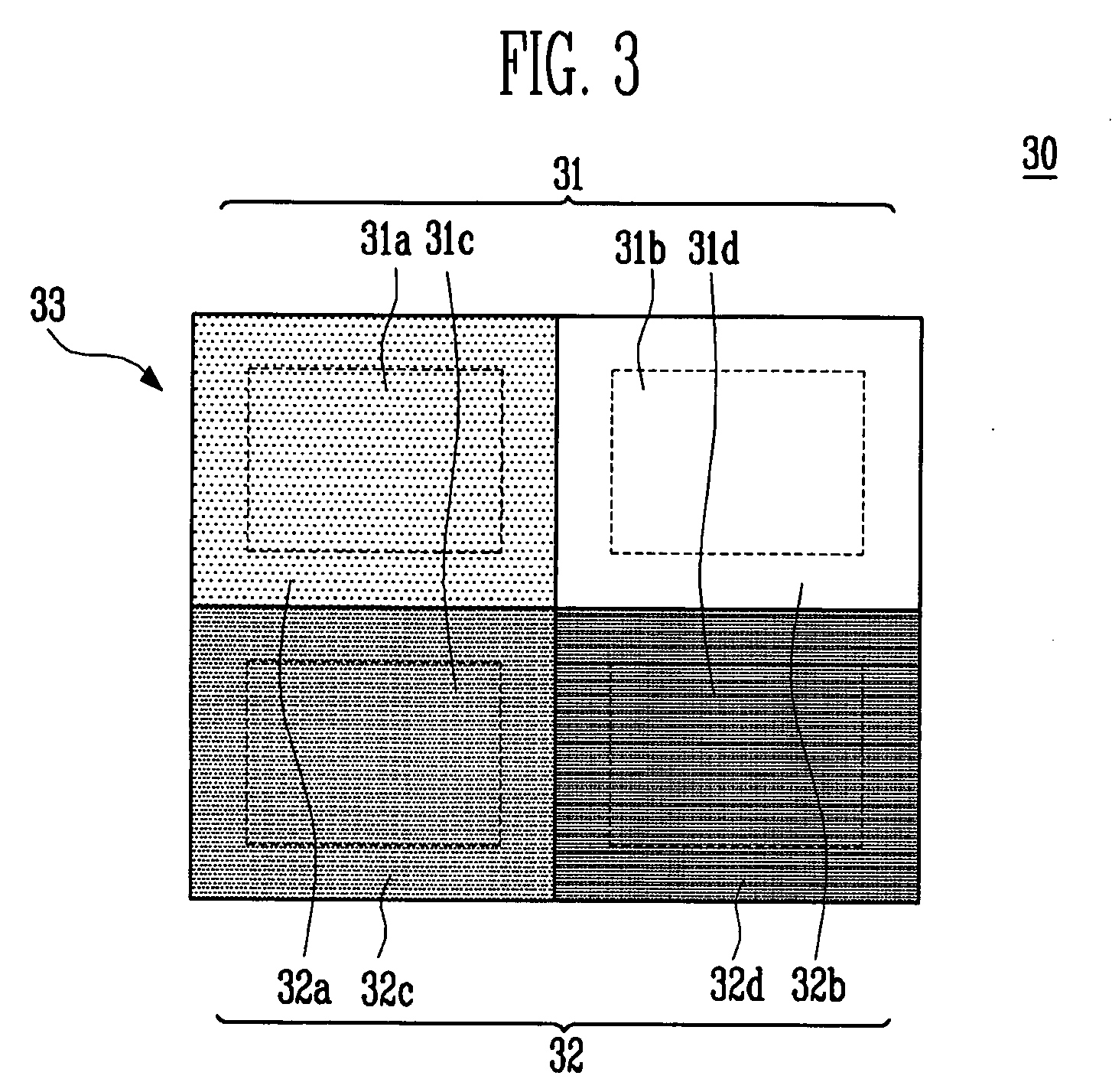
A photo sensor includes a light incidence unit including a plurality of light incidence layers, the light incidence unit having a varying light transmittance with respect to external light, and a photo sensing unit including a plurality of photo sensing elements, the photo sensing unit being configured to output electrical signals in accordance with an amount of light transmitted through the light incidence unit to determine intensity of the external light, each of the photo sensing elements being configured to output electrical signals in accordance with light transmitted through a respective light incidence layer.

Description

BACKGROUND OF THE INVENTION[0001]1. Field of the Invention[0002]Embodiments of the present invention relate to a photo sensor. More particularly, embodiments of the present invention relate to a photo sensor with improved light sensitivity and a light emitting display including the same.[0003]2. Description of the Related Art[0004]An organic light emitting display is a self-emission display exhibiting improved characteristics, e.g., viewing angles, contrast, response speed, power consumption, and so forth, as compared to conventional display, e.g., a liquid crystal display (LCD).[0005]The conventional organic light emitting display may include organic light emitting diodes (OLEDs), i.e., organic light emitting layers between anode and cathode electrodes. The organic light emitting displays may be divided into passive matrix types, i.e., the OLEDs may be coupled to each other between scan and signal lines in a matrix to form pixels, and active matrix types, i.e., the OLEDs may be con...

Claims


Application Information

Patent Timeline
Patent Type & Authority Applications(United States)
IPC IPC(8): H01L33/00H01L31/00
CPCG01J1/02G01J1/0209G01J1/04G01J1/0418G01J1/0488G01J1/4228H01L31/153H01L27/1446H01L27/3269H01L31/02162H01L31/103H01L31/105G02F1/13318H10K59/13H01L31/12
Inventor IM, KI-JUCHOI, BYONG-DEOGKIM, WON-SIKPARK, HYE-HYANGYANG, HUI-WONLEE, YUN-GYU
Owner SAMSUNG DISPLAY CO LTD
Why Eureka
Try Eureka