

Semiconductor photodetector device
a technology of semiconductors and photodetectors, which is applied in the direction of semiconductor devices, radio-controlled devices, electrical apparatus, etc., can solve the problems of preventing sufficient improvement of high-frequency characteristics, deterioration of high-frequency characteristics of photodetectors, and impaired high-frequency characteristics of bipolar transistors b>20/b>, so as to improve frequency characteristics in the third region, reduce power consumption, and improve the effect of frequency characteristics
- Summary
- Abstract
- Description
- Claims
- Application Information
AI Technical Summary
Benefits of technology
Problems solved by technology
Method used
Image

Examples
embodiment 1
[0083]A semiconductor photodetector device according to a first embodiment of the present invention will be described with reference to drawings.
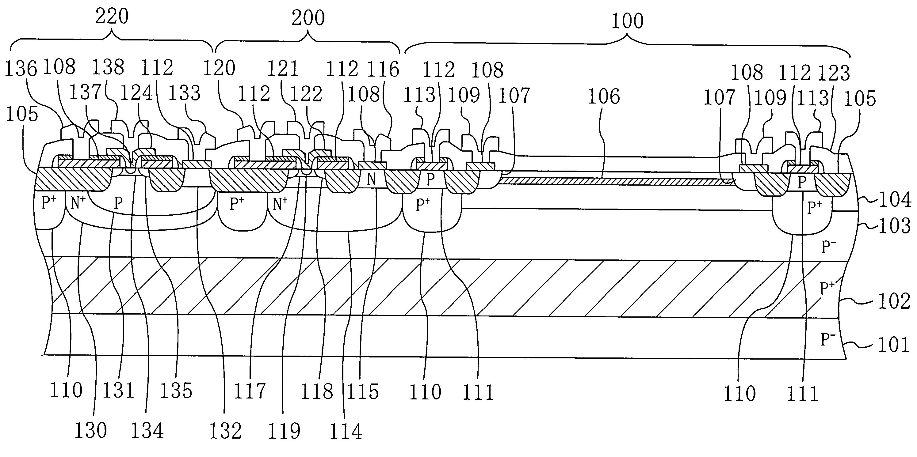
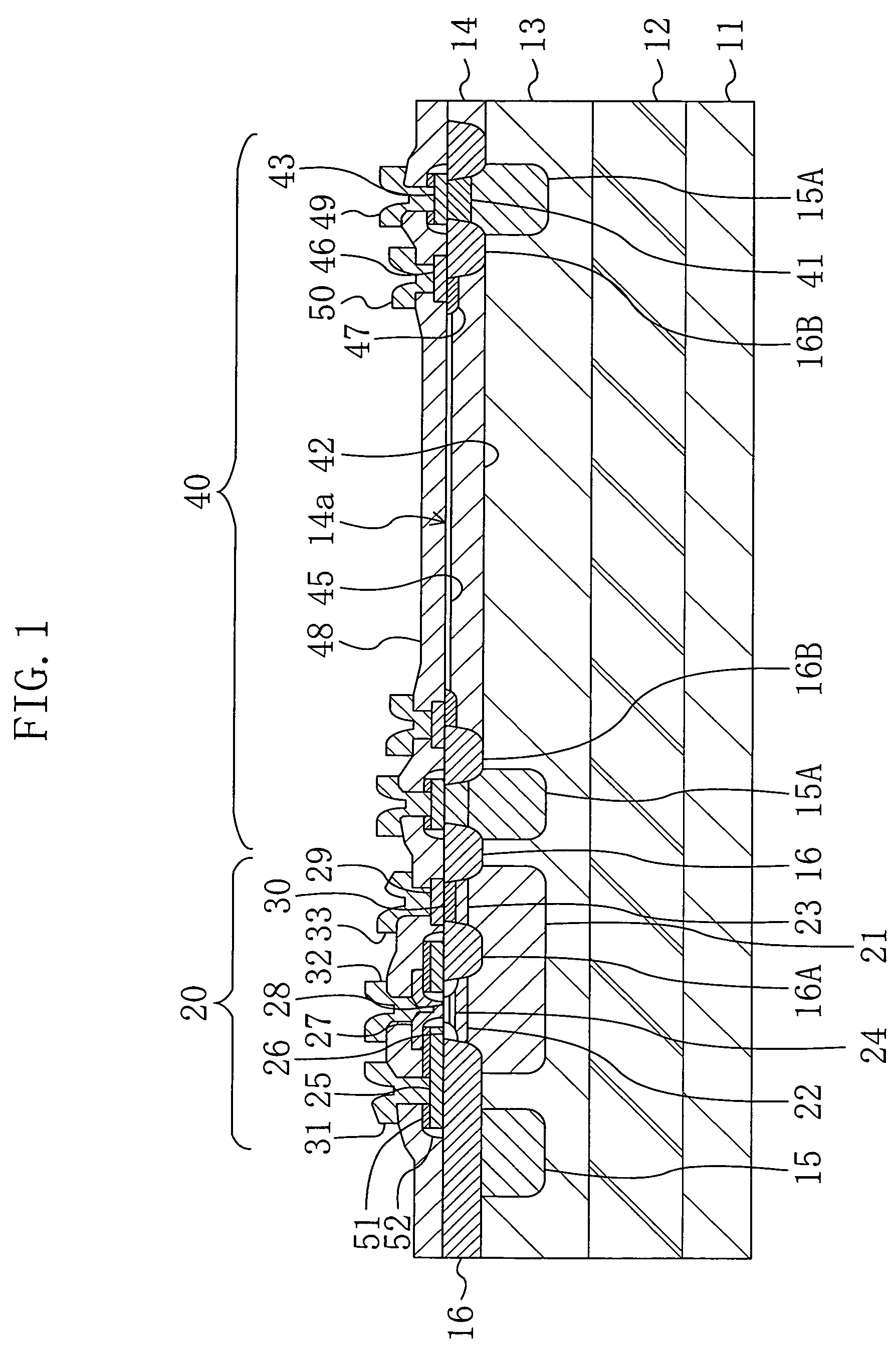
[0084]FIG. 1 shows a cross-sectional structure of the semiconductor photodetector device of the first embodiment. As shown in FIG. 1, a first p-type semiconductor layer (a first region of a first semiconductor layer) 12 containing a p-type impurity at a high concentration, a second p-type semiconductor layer (a second region of the first semiconductor layer) 13 containing an n-type impurity at a concentration lower than that of the first p-type semiconductor layer 12 and an n-type semiconductor layer (a second semiconductor layer) 14 containing an n-type impurity at a concentration higher than that of the second p-type semiconductor layer 13 are formed in this order over a substrate 11 made of p-type silicon. Over the substrate 11, a region where an npn-bipolar transistor 20 is formed and a region where a photodiode 40 of a cathode common t...
modified example 1 of embodiment 1
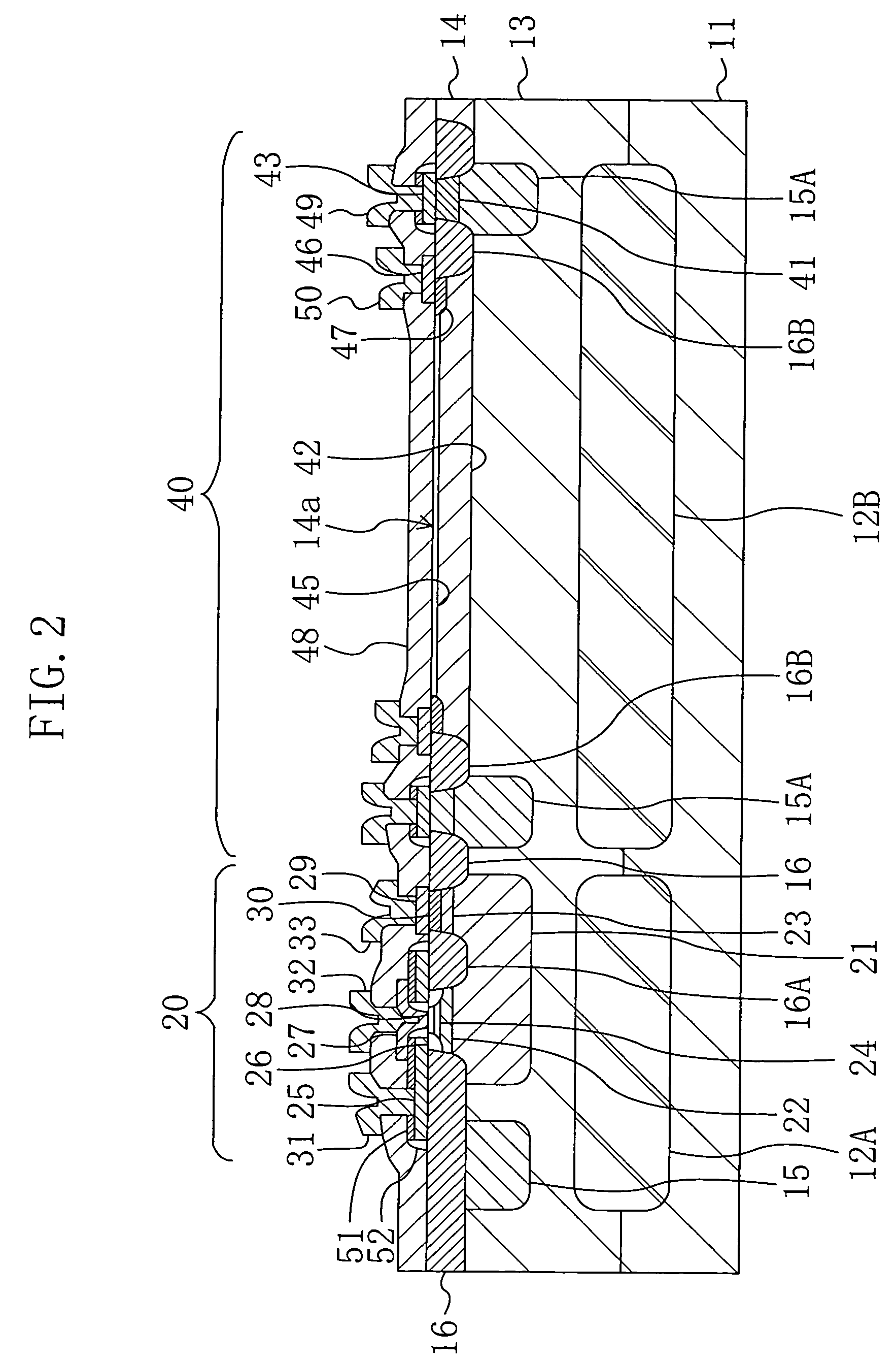
[0101]FIG. 2 shows a cross-sectional structure of a semiconductor photodetector device according to a first modified example of the first embodiment. In FIG. 2, each member already shown in FIG. 1 is identified by the same reference numeral and the description thereof will be omitted herein.
[0102]As shown in FIG. 2, in the semiconductor photodetector device of the first modified example, instead of the first p-type semiconductor layer 12 shown in FIG. 1, p-type buried regions 12A and 12B are selectively formed in a transistor region where a bipolar transistor 20 is formed and a region where a photodiode 40 is formed, respectively.
[0103]In the OEIC device, the bipolar transistor 20 has a circuit configuration in which amplification is performed using a light signal received by the photodiode 40 as an input signal. Accordingly, the amplified signal with a large amplitude is superimposed onto a collector-lower-part extraction region 21, so that parasitic capacitance between the collect...
modified example 2 of embodiment 1
[0106]FIG. 3 shows a cross-sectional structure of a semiconductor photodetector device according to a second modified example of the first embodiment. In FIG. 3, each member already shown in FIG. 1 is identified by the same reference numeral and the description thereof will be omitted herein.
[0107]As shown in FIG. 3, the semiconductor photodetector device of the second modified example is different from the device shown in FIG. 1 in that a bipolar transistor 20 and a photodiode 40 are placed at a given distance from each other and an isolation insulating film 16 has a large width. In this configuration of the second modified example, inductive coupling between the bipolar transistor 20 and the photodiode 40 is reduced, so that it is possible to suppress entering of an alternating current signal amplified by the bipolar transistor 20 into the photodiode. As a result, reduction of the S / N ratio resulting from entering of the signal is also suppressed. The given distance is a clearance...
PUM
 Abstract
Description
Claims
Application Information