Biochip Having Image Sensor with Back Side Illumination Photodiode

a biochip and photodiode technology, applied in the field of biochips, can solve the problems of difficult interlayer dielectric formation and limitations, and achieve the effect of preventing the characteristics of circuits from deteriorating and improving light sensitivity

Active Publication Date: 2011-07-14
OPTOLANE TECH
View PDF1 Cites 16 Cited by
  • Summary
  • Abstract
  • Description
  • Claims
  • Application Information

AI Technical Summary

Benefits of technology

[0015]Accordingly, the present invention has been made in an effort to solve the problems occurring in the related art, and an object of the present invention is to provide a biochip having an image sensor with a back side illumination photodiode structure which can directly collect light with biochemical reaction information, emitted from a biochip layer, so as to improve light sensitivity, and can prevent the characteristics of circuits from deteriorating due to surface treatment conducted during a manufacturing procedure of the biochip layer and infiltration of a solution occurring during a biochemical reaction procedure.

Problems solved by technology

As a consequence, problems may be caused in that it is difficult to form the interlayer dielectric and limitations may exist in performing the surface treatment for the biochip layer and using reacting solutions, etc.

Method used


Image

  • Biochip Having Image Sensor with Back Side Illumination Photodiode

Examples


Embodiment Construction

[0020]Reference will now be made in greater detail to a preferred embodiment of the invention, an example of which is illustrated in the accompanying drawings. Wherever possible, the same reference numerals will be used throughout the drawings and the description to refer to the same or like parts.

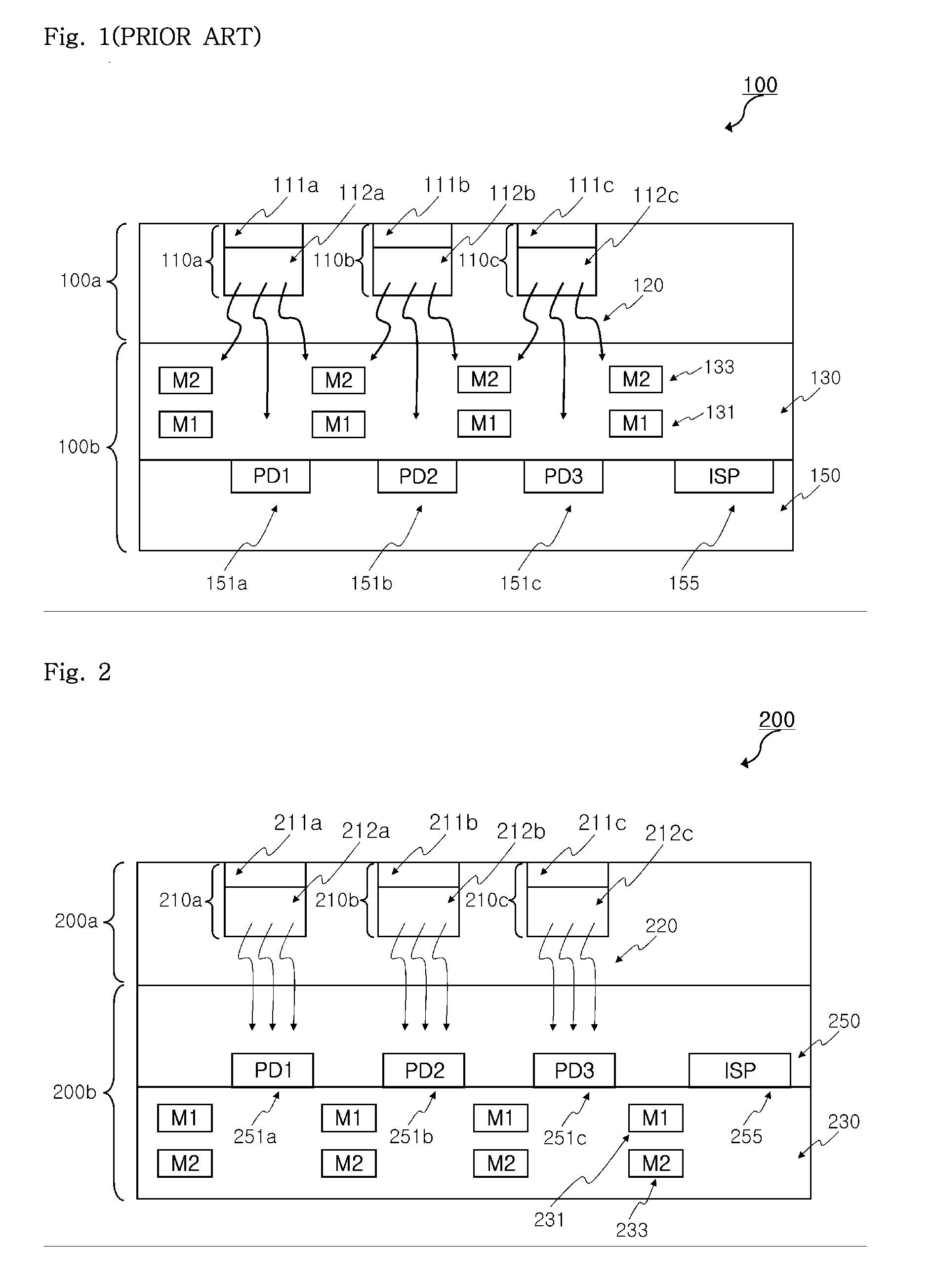
[0021]FIG. 2 is a view illustrating the configuration of a biochip having an image sensor with a back side illumination photodiode structure in accordance with an embodiment of the present invention.

[0022]Referring to FIG. 2, a biochip 200 having an image sensor with a back side illumination photodiode structure in accordance with an embodiment of the present invention includes a biochip layer 200a and an image sensor layer 200b.

[0023]The biochip layer 200a has a plurality of first reaction region 210a, second reaction region 210b and third reaction region 210c which have shapes of grooves.

[0024]The first reaction region 210a has a target sample 211a in the upper portion thereof and a ref...


PUM

PropertyMeasurementUnit
luminescentaaaaaaaaaa
fluorescentaaaaaaaaaa
fluorescenceaaaaaaaaaa

Abstract

A biochip having an image sensor with a back side illumination photodiode structure includes: a biochip layer; and an image sensor layer attached to one surface of the biochip layer and configured to sense light with biochemical reaction information, which is emitted from the biochip layer, wherein the image sensor layer includes a plurality of light sensing parts which receive the light directed toward a back side of a wafer.

Description

BACKGROUND OF THE INVENTION[0001]1. Field of the Invention[0002]The present invention relates to a biochip, and more particularly, to a biochip having an image sensor with a back side illumination photodiode structure which collects light from the back side of a wafer in order to improve capability of sensing light emitted from reaction regions of a biochip.[0003]2. Description of the Related Art[0004]In general, a biochip is manufactured in a type in which reference samples constituted biological molecules such as DNAs, proteins and the likes are regularly arranged on a substrate made of a material such as glass, silicon and nylon.[0005]Biochips are divided into a DNA chip, a protein chip, and so forth, depending upon the kind of reference samples to be arranged. Basically, a biochip uses biochemical reactions between reference samples and target samples which are fixed with respect to a substrate. Representative examples of the biochemical reactions between the reference samples a...

Claims


Application Information

Patent Timeline
Patent Type & Authority Applications(United States)
IPC IPC(8): C40B60/12
CPCG01N21/6454H01L27/14603H01L27/1464H01L27/14627H01L27/14621
Inventor LEE, BYOUNG-SULEE, DO-YOUNG
Owner OPTOLANE TECH
Why Eureka
Try Eureka