Precise metrology with adaptive milling

a technology of precise metrology and adaptive milling, applied in the field of precision metrology with adaptive milling, can solve the problems of hardware limitation of the accuracy with which the initial cut or trench can be placed, and the difficulty of precise imaging of the abs of the pmr write pol

Active Publication Date: 2012-07-17
WESTERN DIGITAL TECH INC
View PDF17 Cites 153 Cited by
  • Summary
  • Abstract
  • Description
  • Claims
  • Application Information

AI Technical Summary

Benefits of technology

[0007]According to another aspect of the subject disclosure, a machine readable medium carrying one or more sequences of instructions for measuring a three-dimensional device in a wafer is provided. Execution of the one or more sequences of instructions by one or more processors causes the one or more processors to perform the step of forming a trench in the wafer. The trench has a facet passing through the three-dimensional device a predetermined offset from a desired image position. Execut

Problems solved by technology

Unfortunately, the accuracy with which the initial cut or trench can be placed is limited by the hardware, and may be sufficiently large to preclude precisely imaging a desired plane.
For example, if the initial placement has an unc

Method used


Image

  • Precise metrology with adaptive milling
  • Precise metrology with adaptive milling
  • Precise metrology with adaptive milling

Examples


Embodiment Construction

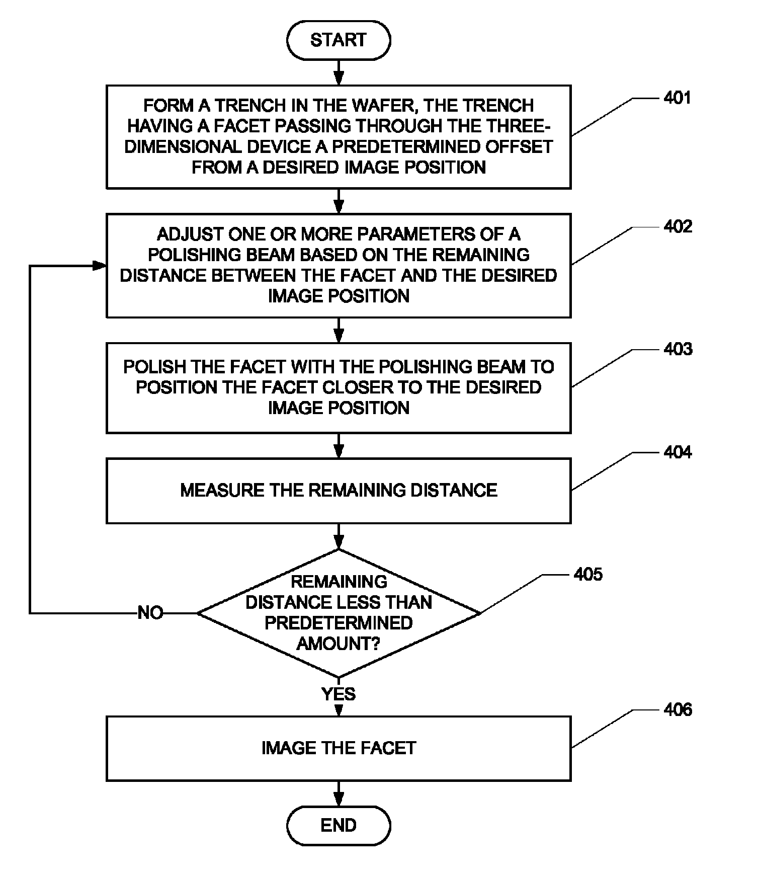
[0016]In the following detailed description, numerous specific details are set forth to provide a full understanding of the present invention. It will be apparent, however, to one ordinarily skilled in the art that the present invention may be practiced without some of these specific details. In other instances, well-known structures and techniques have not been shown in detail to avoid unnecessarily obscuring the present invention.

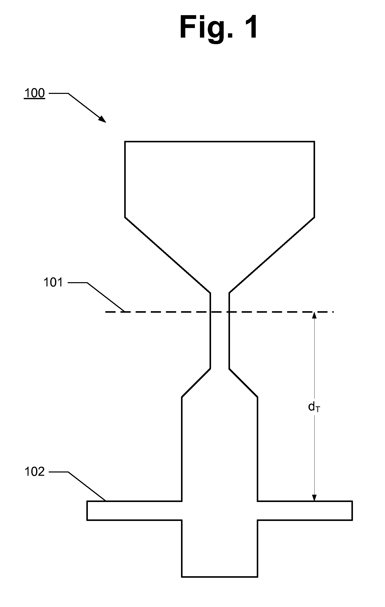
[0017]FIG. 1 illustrates an overhead view of a three-dimensional device 100 in a wafer in accordance with one aspect of the subject disclosure. In the present exemplary embodiment, device 100 is a PMR write pole for a magnetic recording device. Device 100 includes an air bearing surface 101, at which a cross-sectional view of device 100 is desired (e.g., to determine a geometry thereof). Device 100 also includes a fiducial structure 102 a known distance dT from air bearing surface 101.

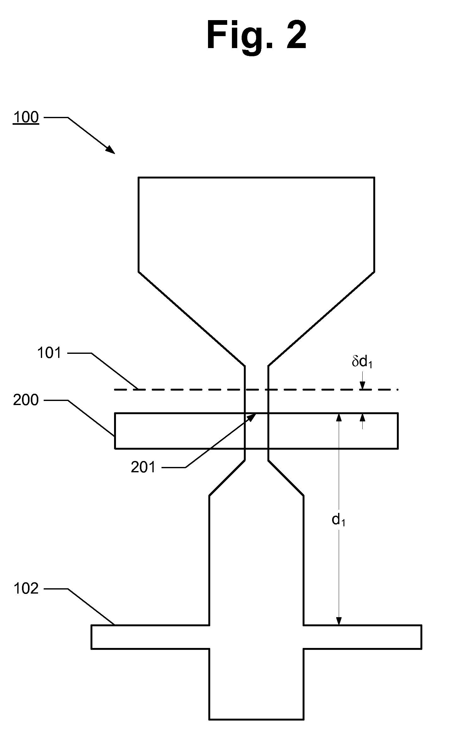
[0018]As the distance between fiducial structure 102 and air bearing su...


PUM


Abstract

A method of measuring a three-dimensional device in a wafer is provided. The method comprises the step of forming a trench in the wafer. The trench has a facet passing through the three-dimensional device a predetermined offset from a desired image position. The method further comprises iteratively, until a remaining distance between the facet and the desired image position is less than a predetermined threshold, adjusting one or more parameters of a polishing beam based on the remaining distance, polishing the facet with the polishing beam to position the facet closer to the desired image position, and measuring the remaining distance.

Description

FIELD OF THE INVENTION[0001]The present invention generally relates to metrology and, in particular, relates to precise metrology with adaptive milling.BACKGROUND OF THE INVENTION[0002]The performance of many devices that are fabricated using semiconductor methods is critically dependent upon the three-dimensional (3D) structure thereof. For example, the performance of a perpendicular magnetic recording (PMR) write pole is highly dependent upon the 3D shape of the write pole near the air bearing surface (ABS), the nose length, and pole flare and / or pinching. To obtain information about the efficacy of manufacturing methods of these and other devices, it is desirable to measure the 3D structure of these devices when comparing the performance of different designs.[0003]One approach to measuring the 3D structure of a device in a wafer involves a “slice and view” (SnV) method employing a dual beam Focused-Ion-Beam Scanning Electron Microscope (FIB / SEM). In this method, the FIB is employ...

Claims


Application Information

Patent Timeline
IPC IPC(8): H01J37/30H01J37/252G01N23/00
CPCH01J37/28H01J37/3056H01L22/12H01L22/20H01J2237/281H01J2237/31745H01J2237/31749H01L2924/0002H01L2924/00
Inventor CHIEN, CHESTER XIAOWEN
Owner WESTERN DIGITAL TECH INC
Why Eureka
Try Eureka