Power semiconductor module comprising elastic housing for accommodating movement of individual substrate regions on a heat sink

a technology of semiconductor modules and heat sinks, which is applied in the direction of semiconductor devices, semiconductor/solid-state device details, electrical apparatus, etc., can solve the problems of low bending stiffness, mechanical stresses in the module, undesirable deformation or flexure at the underside of the substrate or the module, etc., to achieve the effect of reducing the number of rejects in respect of finished modules, increasing yield and improving mechanical deformation

Inactive Publication Date: 2012-07-24
INFINEON TECH AG
View PDF30 Cites 0 Cited by
  • Summary
  • Abstract
  • Description
  • Claims
  • Application Information

AI Technical Summary

Benefits of technology

[0014]Substrates become more sensitive to fracture and damage as their size increases. Therefore, one advantage of the invention consists, moreover, in the fact that the power semiconductor module according to the invention with its plurality of individual substrate regions is significantly more robust mechanically. This advantageously increases the yield in the manufacturing and mounting process.
[0015]A further advantage of the present invention consists in the fact that the individual substrate regions populated with semiconductor components can be individually tested in advance and be replaced in the event of a defect. The rejects in respect of finished modules can thus be minimized in a cost-effective manner.
[0016]This is accompanied by a further increase in the yield, because in the event of defective substrate regions, the entire substrate material associated with a power semiconductor module, if appropriate with the components already mounted, need not necessarily be rejected.
[0017]A further essential aspect of the invention is to be seen in the fact that the substrate regions are connected such that they can move relative to one another via one or a plurality of connecting regions. The respective connecting region has a higher mechanical deformability (elasticity) than the substrate usually has. Thus, as it were hinges or articulated regions are formed between the substrate regions. The connecting regions prevent the substrate regions from having a reciprocal mechanical influence in the adjoining substrate regions.
[0018]Furthermore, at each connecting region there is the possibility of performing a correction in the orientation of the individual substrate regions in such a way that the deformation is minimized and, consequently, a planar contact area of the power semiconductor module is formed, which provides an optimized heat transfer to a heat sink to be connected.
[0019]According to the invention, the power semiconductor module additionally has a housing, which, in the region between the substrate regions, has action points for a mechanical pressure application of the connecting regions, the housing applying pressure to the individual substrate regions.

Problems solved by technology

What are problematic in this case are the mechanical stresses in the module brought about by different thermal expansion coefficients and low bending stiffness of the various module components (e.g. of substrate and semiconductor material).
Mechanical stresses and / or the low bending stiffness may in this case lead to undesirable deformations or flexures at the underside of the substrate or module.
A uniformly planar contact area is then no longer ensured since the heat transfer between cooling element and cooling is impaired by the air gaps and interspaces which arise on account of the deformations.
The aforementioned effects cannot be compensated for particularly where the substrate is not pressed directly, or is pressed only inadequately, onto the heat sink, such as, for example, in the case of edge fixing in the module center, since the flexure (curvature) is greatest there.
However, by virtue of the additional baseplate and the mounting thereof, this construction increases the overall costs of a power semiconductor module configured in this way.

Method used


Image

  • Power semiconductor module comprising elastic housing for accommodating movement of individual substrate regions on a heat sink
  • Power semiconductor module comprising elastic housing for accommodating movement of individual substrate regions on a heat sink

Examples


Embodiment Construction

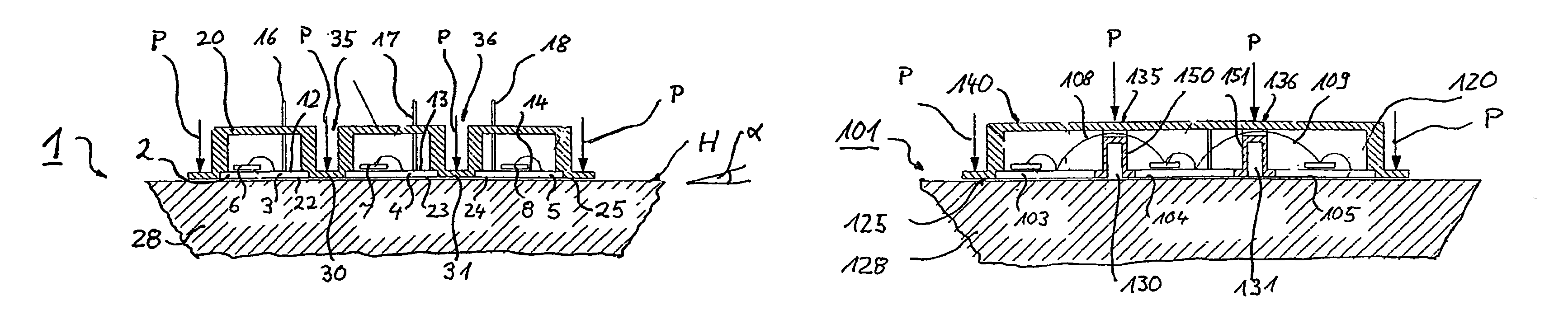
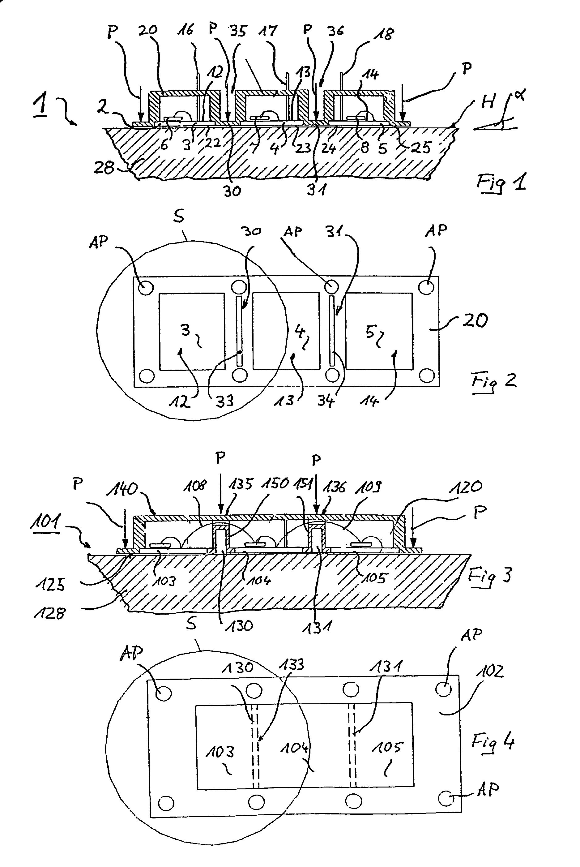
[0032]The power semiconductor module 1 shown in FIG. 1 comprises a ceramic substrate (carrier element) 2, which is segmented into a plurality of substrate regions (partial substrates) 3, 4 and 5 and has as it were three segments S (FIG. 2). Arranged on the substrate regions 3, 4 and 5 are semiconductor components 6, 7 and 8, which are all constituent parts of the overall module 1. The semiconductor components are contact-connected via indicated bonding wires to conductor tracks (not specifically illustrated) which are formed on the respective surface 12, 13, 14 of the partial substrates. The conductor tracks of different partial substrates may be electrically connected to one another via bonding wires. The conductor tracks lead to contact pins (connection pins, 16, 17, 18 for the external connection of the power semiconductor module. The semiconductor components 6, 7 and 8 may be power semiconductors which develop high power losses converted into heat and therefore require an effect...


PUM


Abstract

The power semiconductor module (1) comprises several semiconductor components (6, 7, 8), located on a substrate (2). The aim of the invention is to prevent a reduction in the pressure of the substrate against a cooling surface and the resulting loss of cooling arising from deformations. Said aim is achieved, whereby the substrate (2) comprises several substrate regions (3, 4, 5), with one or several connection regions (31, 32), located between substrate regions (3, 4, 5), by means of which the substrate regions (3, 4, 5) are connected such as to move relative to each other.

Description

CROSS REFERENCE TO RELATED APPLICATION[0001]This application is a continuation of copending International Application No. PCT / EP02 / 09457 filed Aug. 23, 2002 which designates the United States, and claims priority to German application No. 101 42 971.1 filed Sep. 1, 2001.TECHNICAL FIELD OF THE INVENTION[0002]The present invention relates to a power semiconductor module having a plurality of semiconductor components situated on a substrate.DESCRIPTION OF THE RELATED ART[0003]Modules of this type are disclosed for example in DE 39 06 690 A1, DE 199 42 915 A1, DE 197 07 514 A1 and JP 2001118987.[0004]In the case of a power semiconductor module revealed in DE 199 42 915 A1 for example, a plurality of power semiconductors are arranged closely adjacent in a row on the top side of an insulating and thermally conductive carrier (substrate). Said power semiconductors are electrically connected by means of contact areas via metallic conductor tracks formed on the same top side, and can be driv...

Claims


Application Information

Patent Timeline
Patent Type & Authority Patents(United States)
IPC IPC(8): H01L23/10H01L23/36H01L23/31H01L25/07H01L25/18
CPCH01L24/49H01L25/072H01L2224/48091H01L2224/48137H01L2224/49H01L2924/01004H01L2924/01005H01L2924/01015H01L2924/01029H01L2924/01032H01L2924/01033H01L2924/01075H01L2924/01082H01L2924/16152H01L2924/00014H01L2924/01068H01L2924/014H01L2224/73265H01L2924/15787H01L2924/181H01L24/48H01L2924/00H01L2224/45099H01L2224/05599
Inventor STOLZE, THILO
Owner INFINEON TECH AG
Why Eureka
Try Eureka